Your basket is currently empty!
Blog
-
Ovation 250 Power Amplifier
The Ovation 250: A 250W per Channel Audio Power Amplifier (updated 1st June 2013). This amplifier was designed and built in 2005/2006 as my first foray back into audio design after a nearly 20-year hiatus, This write-up was originally published in 2009 when I was living in Tokyo, Japan.
Introduction
Diy Audio is a wonderful activity:- if you cannot afford a $10 000 power amp, you can always build one that comes pretty damn close in terms of sonics for a fraction of the price.
In the intervening years between the early 1970’s and the mid 1990’s, some breakthrough’s in amplifier design were made by a number of researchers and practitioners, and this knowledge entered (and is still entering) the audio design mainstream.
In the mid 1990’s, the first edition of Douglas Self’s ‘Audio Power Amplifier Design Handbook’ was published, and has gone on to become it could be argued, the most important introductory text to audio power amplifier design. It swept aside decades of misinformation and nonsense, placing the ‘art’ firmly in the realm of electrical engineering and physics. Thanks primarily to the work of Self, the 8 distortions that plagued amplifier performance, and therefore had a large impact on their measured performance and sound, have been codified and their cures laid out clearly and concisely. Furthermore, a greater understanding of the role feedback and compensation design plays in amplifier sound developed, along with an appreciation of the importance of component selection in achieving the ultimate in sound reproduction.
Execution of the design leading to the final end product is crucial and includes attention to PCB layout and wiring to avoid ground loops and hum; seemingly innocuous things like tapping off the feedback point in the wrong place can result in an 6-8dB increase in distortion, or not following good cable dressing practice leading to magnetically induced noise and distortion.
But audio, like other branches of engineering, also obeys the law of diminishing returns:- if all the rules have been obeyed, then beyond a certain point large sums of money and effort have to be expended to gain only a marginal improvement if any. In well engineered commercial audio power amplifiers, beyond perhaps $3000 or $4000, product aesthetics and ‘sonics’, are the deciding factors – absolute performance specifications differences play very little part.
The Ovation 250 Power Amplifier
The ‘Ovation 250’ was my first foray into power amplifier design after a 25 year hiatus from audio. This is a fully balanced topology amplifier that delivers (on 110/220vac) 280W RMs per channel into 8 Ohms, and about 480W RMS into 4 Ohms. The rise time, with the input filter disabled, is 1.5us (10%-90%) in both the +ve and -ve slopes. Its powered by a 2KVA torroidal transformer I had specially wound for the job – its ultra quiet. The power rails are filtered by 47mfd per rail, and the front end is powered off a zener + pass transistor regulated +-80V rail, whilst the output stage runs on +-70V. Being a low feedback design, distortion is not particularly low, and comes in at about 0.1% THD20. I’m not particularly obsessed with ppm distortion – big, fast amps are what I like.
The front panel has a on/off power switch, a clip LED indicator (one per channel) and two status LED’s covering power and ‘system ok’. Around the back, there are two sets of WBT style speaker connectors for each channel (to cater for bi-wiring), a switched IEC power inlet and 2 phono jack type input sockets.
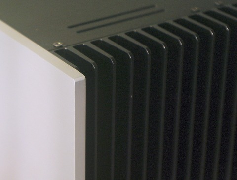
The Ovation 250 weighs in at 38Kg (about 83lbs). There are a few pictures in the gallery.
Ovation 250 Schematics.pdf (updated on June 10 2012)
I originally started looking into this design a few years earlier, and had toyed with single ended to balanced drive and Lin topologies feeding a mosfet (IRFP240/9240) output stage, but eventually settled on a fully balanced (‘FB’) topology using a bipolar output stage based on the MJE21193/4 devices.
Soon after starting this design, I joined diyAudio.com and was introduced to Self ‘s ‘Audio Power Amplifier Design Handbook’ and some very lively discussion around power amplifiers, in the process becoming aware of a lot of new information and techniques. Thus, many of the design aspects are different in some of the designs I am working on now (a 180Watter and another big amp targeting 350W). In those designs, I have retained the FB topology and the bipolar output stage because I am familiar with them and focused on refining the design to improve things like distortion, phase margin and so forth.
My designs feature EF triple output stages and very high slew rates (this is the figure with the front end filter disabled). To achieve this, I run the LTP stage rich at about 10mA (5mA per side) with lots of degeneration, which of course tends to lower the open loop gain, and thus the loop gain. I run the VAS at about 30mA, and when this is coupled to the high input impedance of the EF Triple, the amplifier easily drives complex, heavy loads. In the Ovation amplifier described here, I also loaded the VAS in order to flatten the open loop gain to beyond 20 KHz. Having said that, this is not a technique I have repeated on the subsequent designs, where I have instead used an inner feedback loop (‘Miller Input Compensation’) around the output pre-driver, VAS and LTP to achieve the same thing in the interests of stability, rather than any specific desire to create a wideband open loop design.
The MJE21193/4’s are very rugged 250W transistors with a large SOA, relatively flat Hfe vs. Ic characteristic (though not in the same league as the MJL3281/1302) and they are cheap. The major problem with these transistors though is their rather pedestrian Ft of 4MHz and this translates into stability issues if you try to run with too much loop gain – in a practical design, you will have to run with about 10dB less loop gain at 20KHz than you would with the much faster MJL3281/1302 devices for similar phase and gain margins. This of course translates directly into higher distortion. Big, fast (high SR), wide bandwidth amps sound good and it’s not going from 0.1% to 0.0001% that makes the difference.
Circuit Description
The input is via J7 and into the non-inverting input transistor pair Q18 and Q21 via a 160KHz LPF filter formed by R70 and C19. The input impedance at 1KHz on this amp is about 23k Ohms. The inverting input is formed by Q19 and Q20. All four transistors are degenerated by 150 Ohm emitter resistors (R52-R56). Q16 and Q17 provide the LTP currents which are set at 10mA (so 5mA per side) in this design. This high LTP current, along with heavy degeneration coupled to a low value for Cdom (C29 and C30 at 33pF each), ensures that the input stage can never overload, making this a ‘TIM free’ design. The Ovation 250 was modified in July 2012 for TMC, and this is provided for by the additional 150pF capacitors (C14 and C24) and 1k resistors (R1 and R23).
The balanced output of the LTP pairs are cascoded by Q26, Q27, Q28 and Q31. The front end drive to the VAS stage is developed across R57 and R60 (390 Ohms each). This design does not use mirror loading of the LTP’s, which would raise the loop gain significantly, but require added complexity to overcome the common mode current balance problems (see Edmond Stuart’s write-up’s on this on diyAudio.com). In this design, I returned the inverting LTP outputs to the emitter degeneration resistors (R49 and R51 68 Ohms each) rather than to the rails as is normal practice. This is a trick I saw in a James Bongiorno design and it can offer a few ppm improvement in distortion. The output of the LTP stage feeds a cascoded VAS consisting of Q23 and Q25 in the top +ve half of the VAS and Q22, Q24 –ve bottom half of the VAS. I used legacy BF469/BF470 transistors on this amp which feature very low Cob (critically important for a VAS transistor) and high Vce – I was able to get a whole lot from a work colleague at the time I developed the Ovation 250 in 2007 and early 2007. These transistors are no longer available, and also note that if you try to use them in any LTSpice amplifier simulations, you will get terrible distortion results because the models are not functional. However, in practice, they work just fine.
For the VBE multiplier, also called a ‘Vbe spreader’ (Q15 and Q29 and the associated components), I used a CFP design, because I had concerns that with the relatively high VAS Iq (about 30mA) and possible cross conduction such that at HF, the VAS would ‘open up’ causing serious problems – another reason why the Vbe multiplier is decoupled with a large 33uF (C26). Q15, a BC847C small signal SMD device, is mounted close to one of the output devices collector leads to sense the temperature. I originally thermally coupled this device to the output device collector lead using a blob of heat sink compound, but found that this over compensated the output stage, so as it warmed up, the output stage Iq kept dropping. After I removed the heat sink compound, I got much better results, so that now from cold to very hot, the Iq delta is about 40mA per pair, going from 120mA to 160mA. In my more recent desiogn, the Ovation e-Amp, I used a two point Vbe compensation scheme for better Iq stability over temperature
In the original design, the output of the VAS is heavily loaded with 15k Ohm resistors and I did this after reading an exchange on diyAudio.com about the importance of ‘wide open loop bandwidth’ for good sound. This, coupled with the very heavy front end degeneration, meant that there is a very modest amount of loop gain. Later, I became aware of Robert Cordell’s view about this, and did some further study on the subject and concluded that this in fact was not the case, and as a result removed them, improving the overall loop gain to about 50dB at 1KHz and 25dB at 20KHz, and lowering the distortion by about 12dB. My e-Amp design provides jumper linable loading of the VAS to ground, and this allows me to experiment with loop gain magnitiude simply by inserting or removing jumpers.
The output of the VAS stage feeds a triple emitter follower with Q30 and Q32 operating as class A pre-drivers. I run these at about 10mA by making R65 = 270 Ohms. Originally, I used a speed-up capacitor, C18, across R65, but came to realize that this was not necessary in the pre-driver stage input and removed it. The pre-driver output feeds into the MJE15032/33 (Q13 and Q14) driver stage via 27 Ohm and 1nF RC networks in each driver base. On the original homemade prototype PCB, I could not get rid of the parasitic oscillation in the output stage. After doing some research, I found an application note discussing the oscillation problem on emitter followers and how to cure it. After a bit of experimentation, I settled on the values shown. The -3dB cutoff of these networks is about 5.8MHz, so about an order of magnitude higher than the unity loop gain (ULG) frequency.
The drivers feed into the output stage, and like the pre-drivers, also run in class A and R26 sets the driver stage to about 80mA. This is quite high, and the drivers are therefore co-mounted on the same heat sink as the output transistors Q209 through Q211 (MJL21194) and Q201 through Q205 (MJL21193). In order to tame any parasitic oscillation, each of the output transistors bases has a 3.3Ohm stopper resistor fitted. Although the circuit shows 0.1 Ohm emitter degeneration resistors on each of the output transistors, I actually ended up settling on 0.22 Ohm’s. You need very good thermal compensation and bias stability performance if you are going to settle on 0.1 Ohm output device emitter degeneration devices. Although the Ovation 250 thermal stability is quite good, its not good enough for 0.1 Ohm degeneration resistors. The Iq (adjusted by R2) is set to 120mA per pair (so, 26mV drop across the 0.22 Ohm resistor) after about 15 minutes warm up time.
Basic 2 slope protection is afforded by Q1 and Q7 and the associated components. On my newer designs, I have gon for simple current detection using an opto isolator. I would concede on this design, that the protection is perhaps a little too aggressive.
This design utilizes an output inductor 2uH in the circuit, but later wound for 5uH. With slow output devices like the MJL21193/4, it does not take much capacitive load to pull the output stage pole below the ULG frequency and the consequence is instability or oscillation. The output inductor effectively isolates the capacitive load from the feedback take off point, preventing this problem. However, the low loop gain on this design does mitigate the tendency toward instability with capacitive loads somewhat. Having said that, I really don’t believe a small output inductor is an issue when the speaker cabling inductances can easily reach 4 or 5uH. I originally mounted the Zobel network (R3 and C1) across the speaker terminals, but later wired these directly to the output rail (this is the place where all the emitter degeneration resistors connect together, just before the output inductor. The output of the amplifier is fed to the speakers via 3 16A relays wired in parallel.. I used 3 to ensure low output resistance. On my latest design I have elected to go for a solid state relay based on low Rds(on) 150V mosfets. These are much more reliable than relays when called upon to break high DC currents, as would be the case in a fault condition where, say, one of the output devices failed short to either of the supply rails.
The feedback resistor network values are low, and this is a consequence of running the LTP’s at a high tail current. Although one would expect the input pair base currents to cancel, this does not always happen in practice. I found about 30mV of offset on the output (input LTP transistors not selected), and R31 and associated components (not shown on the circuit) simply allows this to be easily dialed out. I’ve measured the output offset from cold (about 25C) to hot (circa 55C) on two occasions over the last 2 years, and the offset remains below 5mV. No need for servo’s here, and I am confident, with careful layout, this design could be direct coupled and still show very little drift and offset over time once dialed out.
For the control board, I used an NXP 89LPC922 8 bit microcontroller. This connects to each amplifier board via a 20 way ribbon cable, and also provides the high voltage supply for the front end. The controller looks after inrush current limiting (powering up a 2KV transformer without in rush protection trips the mains CB every time), DC offset detection and protection, output stage clipping indicator (this is also handled by the uController) and speaker relay delay’s.
Well, How Does it Sound?
I was in Yodabashi (6 floors of consumer electronics here in Tokyo with some great sound rooms and a big selection of audio) a few months ago and heard a fantastic high end Denon mosfet amp with a big pair of Tannoy speakers. I have never associated Tannoy’s with great sound (apologies to Tannoy fans out there – I have just never heard any prior to this occasion). The imaging was absolutely outstanding (holographic) and top end was smooth as silk, and I thought ‘Wow, that’s absolutely wonderful’. Later that day, I put my system on, dropped a CD in and listened. ‘Wow’, I thought, ‘that’s wonderful too’. It sounded different, but it sounded great. For me, as an audio designer building for myself, that’s what counts – I can have fun designing and building audio gear, and it sounds as good as some great commercial equipment out there!
-
CFA vs. VFA: A Short Primer For the Uninitiated

This article was written in 2014 in response to what can only be described as a vitriolic debate as to what constituted a CFA on diyAudio.com. At the time, many of the participants were struggling to grasp the fundamental differences between VFA’s and CFA’s, and even how to tell them apart. So, this document is not filled with math equations (others have done it already, and done a better job of it than I could ever do) but instead focuses on how they perform differently and how they stack-up against each other in the context of audio amplification. Importantly, it goes on to show that once the designer elects to go for high open loop gains in a CFA design, the resulting behaviour of the CFA morphs into that of a high loop gain VFA, and, whatever topology is used, the output stage is the ultimate arbiter of bandwidth in any practical amplifier.
There are many explanations about IC CFA topologies like this one. Some plunge into math, loop gain equations and so forth, leaving the reader none the wiser, while this one (equations 1~4 and associated gain plots) from Hans Palouda is altogether easier to understand, as is ADI’s here. For VFA, Bruno Putzeys’ explanation is by far the most succinct, even though the main thrust of his article is to dispel some enduring myths about negative feedback. Which brings me to the reason for this short document: ‘CFA vs. classic VFA– a short primer for the uninitiated’ in which I will try to explain the differences between the two topologies, dispel the myths and hopefully encourage more audio power amplifier designers to experiment with this technique.You can download the article here:
An Introduction to CFA Amplifiers for Audio
-
Audio Power Amplifier Design – Peter J Baxandall
In this 6 part series of articles published from January 1978 in the now defunct Wireless World magazine, Peter Baxandall takes the reader through some of the fundamentals of audio amplifier design as they were understood at the time.
Baxandall_Audio Power Amplifier Design
In 1978 there was still much discussion about feedback and how to apply it. Otala’s famous paper about TIM had been out for a few years and some of the assertions in that paper were beginning to be challenged. Solid state amplifier design was still very much a formative discipline with most practitioners trying to see through what appeared to be the conflicting requirements of high feedback, zero TIM, and low distortion. It would be a few more years before the rules of the game would emerge, and designing ‘blameless’ amplifiers became a reality.
-
Douglas Self’s 8 Distortions and a Few More
(pictured above is the hifisonix 180 Watt per channel e-Amp)
No one had codified all the major audio amplifier distortion mechanisms until Douglas Self published the first edition of his ‘Audio Power Amplifier Design Handbook’ or APAD’ as it has become known, in 1996. He used a standard Lin* topology amplifier and then proceeded to show in a logical and easily understood manner, how all of the major distortion mechanisms in audio amplifiers could be reduced to ‘vanishingly low levels’ i.e. parts per million levels. In an industry awash with voodoo engineering claims, he was thus careful not claim his amplifier was the best, but merely that in terms of the whole signal chain from studio microphone to the consumers loudspeaker in a domestic environment, the power amplifier contributed the least distortion. He thus termed his resultant design the ‘blameless’ amplifier. 8 key distortion mechanisms were identified in his book and in the short article you can download below, I’ve described each one, how much distortion it can contribute, and how it can be negated with good design.
Douglas-Selfs-8-Distortions-and-a-Few-More
*Lin amplifier topology is named after Harry Lin, a Bell Research Labs scientist who in the late 1950’s first proposed the now standard three stage Voltage Feedback Topology (VFA) amplifier: Input voltage to current stage, integrator and the output stage buffer. All VFA amplifiers are derived from this basic topology.
-
The Theory of TIM – Matti Otala
Matti Otala follows up on earlier research on the subject of TIM.
-
Some Ideas on Temperature Compensation for Audio Amplifier EF Triples
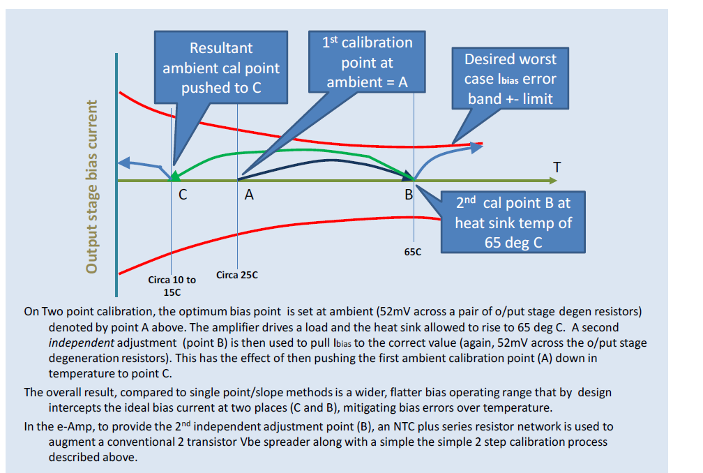
Temperature compensating an EF3 audio power amplifier output stage is not a trifling task. There are 6 Vbe junctions, running at 3 different current densities, different temperatures and neither is the thermal performance of the heatsink assembly characterized in most DIY cases. This makes deploying a conventional 2 transistor Vbe spreader (or Vbe multiplier as it is sometimes called) a little less than straight forward if one is to secure decent temperature compensation – i.e. to within 10% over the full operating range. The article below explores a slightly different approach to the problem in which, during the development phase, the compensation is designed to intersect the ideal bias voltage at two different temperatures, ideally the first at ambient and the second up above 50 deg C – a technique I later called ‘two point temperature compensation’. Some time after writing this in 2010, I started the design and then construction work of the e-Amp, and used what I learned writing this up to solve the problem using an NTD thermistor, which you can read about in the e-Amp article on pages 37 to 40.
-
Review of Bob Cordell’s Book ‘Designing Audio Power Amplifiers’
‘Designing Audio Power Amplifiers’ by Bob Cordell – Reviewed by Andrew C. Russell in 2011
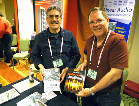
Bob Cordell (on the right) pictured with Jan Didden, publisher of ‘Linear Audio’
After a 15 year hiatus from electronics, I returned in 2005 to linear design not as a professional but as a hobbyist. Earlier in my career, I spent six years designing industrial instrumentation – things like thermocouple amplifiers and linearizers, A-D’s, power supplies, isolation amplifiers and so forth. I’ve always been passionate about music and audio equipment, so it was only a matter of time, with children grown up and out of the home, that these interests would be rekindled.
Audio amplifier design is a specialized branch of electronics in which the engineer seeks to amplify and reproduce very accurately through a speaker system, low level source signals from CD’s, tuners, turntables and the like. As such, it is a fairly unique speciality since it combines precision (very high linearity requirements) over a wide bandwidths (200 to 300 kHz) along with high power requirements (amps of output current with voltage swings of up to +-70 V in a high power unit). Further, with the application of feedback, there is a dash of control theory thrown into the mix as well, and this is especially challenging when one considers that the loudspeaker load is highly non-linear wrt frequency.
Cordell is a professional engineer who has been blessed with the ability to explain complex technical concepts in a concise, understandable manner. This book starts off with the fundamentals of amplification and then goes on to show how to take a basic design, and with a few well-honed circuit approaches, evolve it to create very high performance, low distortion amplifiers. Chapter 5 is an in-depth discussion on feedback and compensation techniques which is traditionally one of the more challenging areas of amplifier design, but he covers this in a practical and succinct manner, exposing even seasoned, professional designers, to an array of advanced compensation techniques.
Voltage amplifier (VAS) and output stage design are also covered, along with the various trade-offs between the circuit approaches and output device technologies (bipolar and mosfet), and associated protection schemes. There is an extensive section on output stage topologies, covering both bipolar and mosfet technologies, along with a very interesting chapter on Hawksford error correction as applied to mosfet output stages, which Cordell helped popularize back in the early eighties with a ground-breaking design at the time.
The book delves into the subtleties of zero global feedback design amplifiers and Cordell diplomatically deals with the debate raging in audiophile circles about feedback (some for, and others against). What is special about this book is that it is grounded in very solid engineering theory and practice, and, rather than express opinions on why a certain design approach or philosophy is best (a temptation most writers and practitioners in the field are unfortunately unable to avoid), Cordell actually covers both sides. The reader thus comes away with an appreciation of the design challenges required in both feedback amplifiers and zero global feedback amplifiers. The same can be said of his discussion around bipolars and mosfets along with output stage protection.
This book is enormously important for the high end audio design community, and makes the state of the art accessible to a whole new generation of practitioners. If you are a professional audio engineer, then this book is an invaluable reference, and will almost certainly help you raise your game. On the other hand, engineering students will find the practical, down to earth explanations a useful resource in helping get from classroom theory into practical designs. And, for a DIY’er, I’d say it is an absolute necessity if one is to gain a solid, clear and unbiased introduction to the art. If Douglas Self is to be credited with removing the misunderstanding around power amplifier design, then Bob Cordell must be credited for bringing state of the art design techniques to within the reach of everyone with any interest in high performance audio in a thoroughly practical and highly readable book.
Highly recommended
-
Saturn V Rocket Performance Report
Absolutely nothing to do with audio, but a great read for the techies.
This performance report was pulled together in the late 1960’s by Walter Haeussermann , one of the German rocket scientists who went to the US after WWII, where he settled and went on to have a spectacularly successful career with NASA. He was a key member of Werner von Braun’s team that made the 1969 US moon landing a reality. Just take a look at the section on the control computer they used to guide the beast . . .
Here is a link to a very nice YouTube video about the Saturn V control and guidance computer https://youtu.be/dI-JW2UIAG0
-
CFA Diamond Buffer IPS: Does it Operate in Class B or class A?
There is a persistent assertion by small group of amplifier design practitioners that the diamond buffer input stage of CFA audio amplifier operates in class B (or AB) mode wherein there is a hard ‘handover’ between each half of the diamond buffer input stage as the input signal passes through 0V. The most recent claim of this kind is in the June 2017 issue of AudioXpress by M. Kiwanuka .
The short article below explores this subject and finds that the claim is wholly incorrect: the front end of a CFA diamond buffer input stage operates well within the class A region for all known audio signals
You can download the article here:- CFA Front End
Note that this article discusses discrete audio power amplifiers and not IC CFA operational amplifiers which are severely power constrained by design.
-
Barney Oliver: Crossover Distortion in Class B Audio Amplifiers

This is the famous analysis of class B amplifier cross-over distortion by the then head of HP Reasearch Labs, Dr. Barney Oliver, published in the February 1971 edition of the HP Journal. The bias current Iq for a class B emitter follower amplifier is shown to be approximately Iq = .026/(Re+re+(rb/hFE)). In practice, – the ideal value ending up somewhere between a 13 to 26mV drop across the output transistor emitter degeneration resistors. This paper provides the theoretical underpinings for that relationship. So, when you hear about the ‘Oliver’ voltage, you know where it came from. You can read more about Barney Oliver here and here
Download the PDF here: Cross Over Distortion in Class B Amplifiers
See the comments below. My practical experience over many amplifier builds is that indeed somewhere 13 and 26 mV is ideal.