Your basket is currently empty!
Blog
-
More Notes On Cascode Amplifier Oscillation
Here is a short write up on cascode oscillation I did back in 2012 when designing and developing the e-Amp.
Cascode Oscillation in Audio Amplifiers.pdf
I recently (2017) had a recurrence of the problem on another high power design – some pictures are shown below. When I went back and looked at the notes above, I realised I had not followed my original advice, and the problem had returned to plague me – clearly a case of ‘those that fail to learn from their mistakes are condemned to repeat them’.

This is what you get when you place the scope probe on the emitter of the cascode transistor. The probe capacitance is probably contributing to the problem and causing it to break into oscillation, or it may be increasing the level of existing oscillation. Either way, its not acceptable, and especially so if you are trying to design a circuit to deliver single digit ppm distortion performance.
Here it is with the time scale expanded:-

If you want to prevent or limit the probe from affecting the circuits behaviour, one trick is to look at it with a 10x probe – the input capacitance is much lower. Another option on 1x, is to place a 50-100 Ohm resistor in series with the probe – this helps to isolate the probe capacitance although you will still have some attenuation because of the scope probe and scope input capacitance. Use a 1206 surface mount device and solder it upright on the node you want to probe. Note that a 1x scope probe input capacitance is about 50 pF//1MEG Ohm and a 10x probe is 15 pF//10 MEG Ohm.
Its very important to note that you can form Colpitts oscillator structures in the base, emitter and collector circuits of transistors. Small signal audio transistors have fT’s of 100 ~ 300 MHz so all you need is some inductance (on a PCB this is often in the 40-60 nH range corresponding to 4-6 cm trace lengths) and then capacitive coupling (10-30 pF – layout dependant) from each end of the inductance to a non-inverting terminal on your amplifying device along with some gain. Below is a screen shot of three circuit examples. They all show HF instability and oscillation to some degree with 10’s to 100’s of mV at 20 to 100 MHz frequencies, but with some value combinations, it is quite easy to get volt level HF oscillation. As you can see, the LC networks that lead to problems can arise across any two terminals.

Although the PCB traces in a conventional analog amplifier are unlikely to be long enough to qualify as antenna’s at the frequencies mentioned, you will still couple a lot of this garbage capacitively into other small signal parts of your circuit. As noted above, if you are working on high performance audio circuits, problems like this will quickly put paid to any ppm or sub-ppm distortion aspirations you may harbour.
The high voltage PNP MMBT5401 and its NPN counterpart the MMBT5551 are often used for level shifters and feature an fT of 100 MHz to 300 MHz and a Cob of 6pF – they are fast and in the cascode configuration will easily oscillate if the conditions are right.
The following preventative measures (not an exhaustive list) provide a good starting point:-
- Place a 470 to 1k SMD (1206 or 0805) resistor as close as possible to the base of the cascode transistor. This lowers the Q of any inductance (i.e. ‘dampens’ it) in the base circuit and swamps any -ve resistance reflected into the emitter.
- In some cases, a SMD ceramic capacitor from the base of the cascode transistor to ground may help. I’ve found values between 10nF and 100 nF work well. Do not use film or anything else exotic – XR7 dielectric rated at 3-4 times the voltage on the base is about right. The capacitor ESR is also part of the fix.
- Make sure the overall loop area from the cascode base reference voltage to ground and the driver transistor in the emitter is small. If not, you will simply be adding inductance in the base circuit and will exacerbate the problem – loop areas have to be kept small to minimize inductance.
- Following on from (3) above, recall that the output at the cascode transistor collector is a current, so you can run fairly long traces from the cascode collector to the next part of the circuit – typically a common emitter stage referenced to the supply rails. However, you must minimize any capacitive coupling from the cascade collector circuit to its emitter – the best way to do this is through attention to layout.
- If the signal currents are low (1~10 mA), the propensity for the cascode circuit to break into oscillation can be further reduced by inserting a resistor of 100 Ohms to 1k in the collector of the cascode, located as close as possible to the device. This technique also helps by the way in emitter followers or beta helpers.
- If your circuit currents are low enough to allow, insert a low value resistor (100~200 Ohms) in the trace close to the cascode transistor emitter – this will help reduce the Q of the trace inductance.
- Pay attention to layout during the design stage – keep the cascode, driver transistor and associate circuit compact and with short traces. Keep loop areas small.
One final point about using Zener diodes as the reference voltage to the base of the cascode transistor. Zeners above about 7 V generate a lot of broadband noise right up into 100’s of MHz. Without filtering, damping and careful layout as described above, this noise can promote instability in cascode circuits.
-
Baxandall’s Original Tone Control Article from Wireless World 1952
This article was published in October of 1952, when Baxandall was 31 years old, the design having already won him a prize 2 years earlier in a competition. His design basically relegated other tone control circuits to the scrap heap, although cheap passive, or non-inverting circuits still persisted well into the 1980’s, especially in low cost mass market products from Japan. Of course, now tone controls can be implemented digitally, but for the analog type, this remains the gold standard.
-
Stan Curtis 60W Class A Amplifier from ETI
Stan Curtis was involved in both engineering and management roles in companies like Quad, Cambridge, Rotel (a family owned Japanese brand) Mission and Lecson to name a few. He is primarily an audio business consultant and remains highly respected and a noted product designer within the sector in his own right.
This is his 60 Watt DIY class A amplifier published in ETI in 1985 which has been referenced on numerous web sites and publications over the last 25 or so years. It’s a rather complex design, but, 60W of class A power translates to a BIG amplifier with significant standing dissipation.
-
Low Cost Isolation Amplifier for Industrial Applications
A Design Idea of mine that appeared in EDN around 2000. The article appeared with the title ‘Lost Cost . . . ‘ – seems someone got a bit mixed up. The idea has been referenced in a few papers on the web – always good to see!
Low_cost_isolation_amplifier_suits_industrial_applications
Here’s another one using a delta modulator that also works very well. I submitted this to EDN but it was rebuffed. I guess whoever reviewed the idea wasn’t used to seeing an opto operated in photo-diode mode.
Another Low Cost Isolation Amplifier for Industrial Instrumentation Applications
-
Hifisonix UBx Universal JFET Buffer
A while back, one of the diyAudio forum members who was building the nx-Amp (here’s the thread on DIYaudio.com) enquired about either reducing the amplifier’s overall gain, or providing a volume control facility. Since both the 15 W class A sx-Amplifier and its bigger 100W sibling the nx-Amplifier, are Current Feedback Amplifiers, performance is quite carefully optimized for a specific gain – they are not as tolerant as voltage feedback amplifiers in this regard. Although not specifically raised in the thread, a consensus seem to develop that what was actually needed was a general purpose buffer that would accommodate the input from a pot, and be able to comfortably drive a power amplifier with typical input impedance of 10 k Ω.
No originality is claimed – Nelson Pass’s B1 buffer has been around for years and is well regarded – the UBx ‘Universal Buffer’, as this will I hope come to be known, also uses this classic configuration (but without the cascode), which I believe was first published by either Siliconix or National Semiconductor way back in the late 1960’s.
You can download the PDF file here UBx
-
OPEX-1: A Discrete OPAMP for Audio
This design showcases a discrete opamp for audio applications. It features very low noise, low distortion and a class A output stage that will deliver 1ppm distortion into a 600 Ohm load at 12 V peak.
-
Solid State Relay with PCB Layout
A complete relay that is smaller than a Tyco RT series EMR Simple_solid_state_relay_Updated . This design uses a small double sided PCB and some SMD components. Here are the Gerber files SSLR. The recomended mosfets for this design are the PSMN4R3-100PS[1] for supply rails of up to +-50 V absolute maximum, and for supply rails of up to +-75 V, the Fairchild FDB075N15A[1]
-
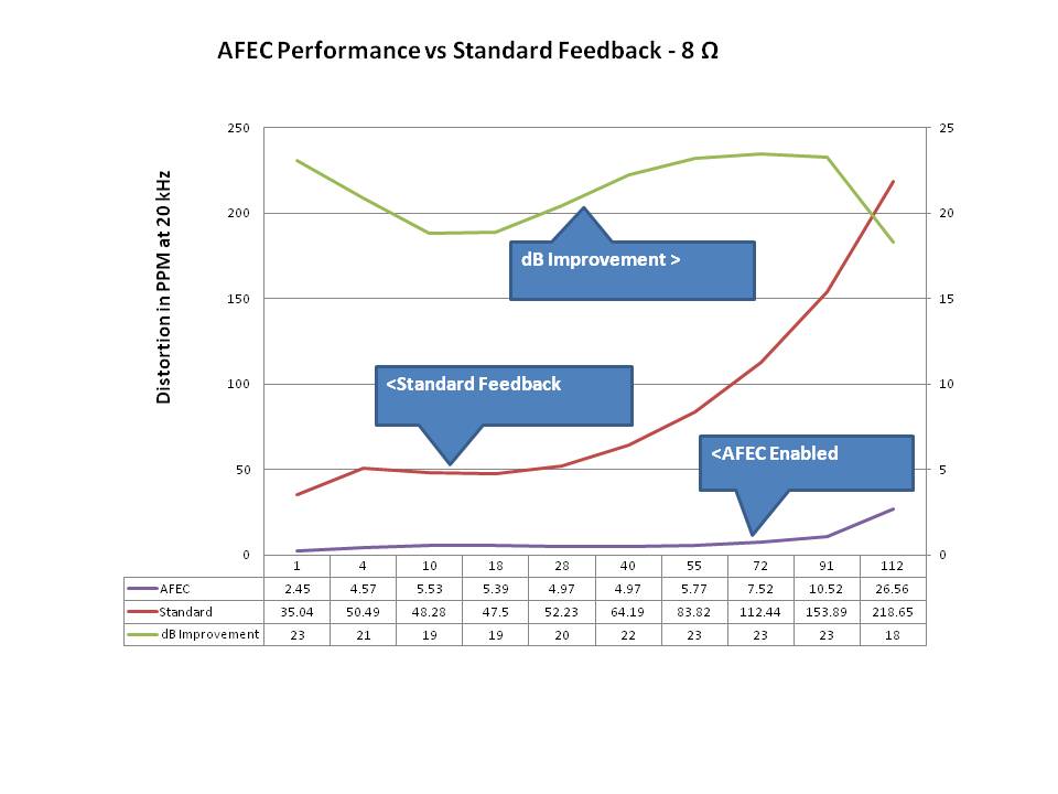
Augmented Feedback Error Correction (AFEC)

AFEC is a simple technique that augments the feedback of an amplifier to dramatically improve the Large Signal Non-linearity (LSN) distortion performance by up to 20 dB across the audio band. Additionally, AFEC acts to remove any DC offsets and also improve PSRR significantly.
Augmenting the feedback in a manner similar to that described in this document has been tried previously – the first example is from the early 1980’s at Hitachi. However, the technique never entered the mainstream – one can only postulate that lack of very high performance opamps (bandwidth, SR and distortion performance), along with the difficultly of being able to characterize such a system for stability modeling purposes (as we can do now on LTspice for example) were contributing factors to its early demise. However, as of 2012, these problems are now solved, so perhaps we shall now see the return of AFEC as a viable distortion reduction technique.
You can download the article here AFEC-V3.0
Excerpt
One of the advantages of CFA power amplifiers is their very high slew rates (200+ V/us is not uncommon), but loop gains tend not to be as high as VFA topology designs. This is fine at low to medium signal levels, where the very good front end linearity and wide loop gain bandwidths of CFAs’ manifest as low distortion; however, at higher power output levels where the output stage and TAS/TIS LSN starts make itself felt, CFA distortion is generally worse, and this is as a direct result of the lower loop gains – note, I am talking here about minimalist CFA topology designs. Cross over is the major type of distortion in class AB amplifiers and there have been various schemes invented to deal with this over the years – most relying on feed forward techniques (see Peter Walker’s Quad Current Dumping for example, or Michael Renardson’s MJR7 design). AFEC does a good job of reducing cross over distortion artifacts, and in particular, those arising from OPS bias current shifts, but it will not compensate for an under biased OPS where there is a clear discontinuity in the crossover region. CFA amplifier PSRR is lower than VFA. This usually necessitates a front-end stage regulator – but even then, the best designs are still usually 20~30 dB below that of VFA exemplars. It will be shown that AFEC can improve CFA PSRR such that it matches or exceeds VFA PSRR, whilst at the same time removing any output offsets as a result of the servo action of the AFEC control amplifier.
-
Output Coupling Inductors
Inductors on the output of an amplifer are used to isolate the amplifer from capacitive loads at HF and ensure stability. There has been quite some debate on DIYaudio.com as to whether they are audible, necessary, or just the result of designers being overly cautious. Some very well known designers in the field have decided against using output inductors. In this short presentation, I explore the pros and cons.
-
Oscillation Sniffer
No ‘scope? This simple circuit can help you quickly see if you have any oscillation problems on your opamp or amplifer circuit.
Note, its NOT designed to be connected to high impedance nodes.


