Your basket is currently empty!
Blog
-
Technical Requirements of Phono Preamplifiers by Tomlinson Holman

Technics Direct Drive Turntable (Photograph by David Gallard) The two articles below were written in the 1970’s, nearly a decade before the arrival of the CD and the ‘perfect sound forever’ claim made by Philips. There was a lot of focus on phono amplifier performance at the time which it could be argued was triggered by the arrival of very high performance turntables – the Linn Sondek and Japanese Direct Drive systems from Technics for example – but there were others like Micro Seki, Thorens and so forth as well. These turntables were for the most part, quiet with low motor noise and decent quality pickup arms.
The arrival of Quadraphonic systems required much greater bandwidths and this had to be matched with improved cartridges that offered better tracking performance and a newer, greater understanding of the electro-mechanics of the pickup itself, and in particular the stylus, emerged as a result.Holmans first article investigated the dynamic requirements of phono amplifiers and represented the best effort at the time – and probably still so – to understand the absolute outer limits of phono amp overload requirements. The general consensus that was cemented from this work, and that of other investigators and cartridge manufacturers at the time (Shure being chief amongst them) was that a typical phono amp should deal with peak outputs of at least 25cm/sec (5cm/sec being the nominal output). This of course does not include factors like ‘hot cartidges’ providing 6-10mV re the nominal 5mV output levels and ‘hot recordings’ where the general levels on the disc, and associated peaks, were higher than average. On top of this, overhead for the inevitable crackles and pops was also required.
The second article presents a practical MM design which should be read in the context of the available semiconductor devices at the time.
-
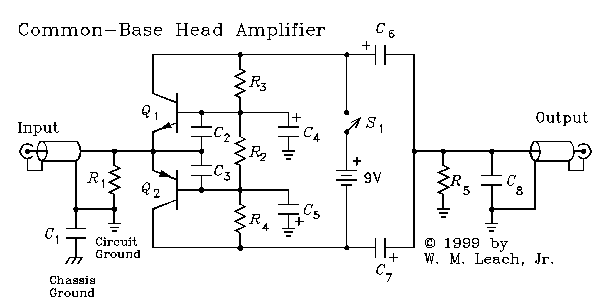
Richard Lee’s Ultra-Low Noise MC Head Amp
This design was a development of Marshall Leach’s MC head-amp, from the 1970s, and to my knowledge, Richard Lee’s implementation presented here has not been bested in terms of noise – about 280pV/rt Hz in a well-implemented exemplar – other than in the Hifisonix X-Altra MC/MM Phono Preamplifier. Importantly, it requires only about 12mA current in the +-15V rail powered version, and about a quarter of that in the battery version. If you try to achieve this type of performance with single-ended designs using PNP devices (the Diodes Inc ZTX951 being an excellent candidate), you will probably require 10 times the current of the battery-powered version or an opamp and a lot more circuit complexity.
The original design back in 1980 was housed in a discarded ‘Duraglit’ tin (a type of polish in the UK used to burnish soft metals like brass, aluminum or pewter), and this design has thus become known amongst the DIY fraternity as ‘Richard Lee’s Duraglit Special’
The design is not without its foibles in that it requires low rbb’ NPN-PNP complements, now (2019) difficult to get (other than the excellent Zetex ZTX851/951 types) and the gain is dependent upon the cartridge DC resistance – so you have to select the output load resistor appropriately. Nevertheless, it is a fantastic example of the ‘less is more’ dictum and achieves remarkable performance for pennies.
Lee worked for various UK Hi-Fi outfits in the heyday of home audio in the 1960’s through 1980’s, including a stint at KEF and is now retired to Cooktown, Queensland, Australia where he relishes living as a ‘beach bum’ (his words, not mine!).
-
My Loudspeakers
I bought a pair of B&W 703’s in about 2003 and they travelled with me all around Asia when I worked there as an expat for ten years. These are big loudspeakers with fantastic bass and mid-range articulation.

The treble may be a little forward for some, but for Jazz, big band and rock they are absolutely superb – exciting, visceral and sonorous . I would describe the sound as effortless with a slightly forward treble balance and they can go very loud. They image well and the bass is crisp, clean and goes very deep. They are an easy load to drive with sensitivity specified at 89dB/W. If you hunt around on the web, you can still pick up an imaculate pair for about $1500 in the US or about £1000 here in the UK. Here’s a review from 2009
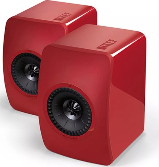
The second pair of speakers I have are the highly regarded KEF LS50’s I purchased in 2017. These are near field monitors and in a small room are unmatched insofar as accuracy of reproduction and stereo imaging are concerned. My music space is quite large, so I cannot listen use them in near field mode, but the imaging and overall balance is still fantastic.

They do not go deep in a big space, although if placed near a corner (500mm – not closer) or wall, the additional acoustic reinforcement does extend the bass down considerably. I use a B&W ASW60 sub-bass that augments them below 80 Hz to flatten the response down to about 35 Hz. I use these speakers to listen to classical music, acoustic and jazz. If you have ever been to a classical concert, when you listen to these speakers, you will appreciate how accurate they are, and how well they image (much better than the 703’s which are not too shabby in this area either). You can read the Stereophile review here and another review here.
More recently, I bought a pair of Dali Oberon 5’s for the living room (the speakers above are in my music room), powered by one of my commercial products, the Model 1707 integrated amplifier. The Oberon 5’s have received rave reviews (here’s another one) since their introduction in late 2019. For the £749 asking price new, these are amazing loudspeakers. Not a hint of sibilance, fantastic imaging to boot and an open, warm sound. They’re compact and well built and will fit in with almost any decor. If you are looking for a pair of speakers to fill a medium sized listening space and don’t want to break the bank, I highly recommend you audition a pair.

-
The Endless Semantic Debate: Current and Voltage Feedback Amplifiers
It seems some are still agonizing over the ‘current feedback’ versus ‘voltage feedback’ definition. Clearly a case of people wanting to continue to flog a horse that was laid to rest five decades ago during the heyday of the analog computer, or they simply fail to grasp the CFA concept. I suspect there are an equal number of both types. This is the same crowd that deny the existence of CFA’s, claiming they are just ill-designed VFA’s. Here then is the question that vexes the CFA doubting Thomas’s:-
What do we call an amplifier that actually has current feedback?
Lets consider this whole current feedback thing by first making clear there are two very different issues to consider here: current output and current feedback and the voltage mode equivalents, voltage output and voltage feedback. Output mode and feedback mode are emphatically not the same thing, and anybody who makes this claim is simply playing word games to further their dogma. Quite depressing, given we are talking about an engineering discipline here – namely electronics.
You can use either a voltage feedback (VFA) or a current feedback (i.e. CFA) amplifier to control its output as either a voltage or a current.
A current output amplifier is an amplifier in which the output current is the controlled parameter. Example: a 4-20 mA industrial loop where the load resistance or impedance can be changed, but the current remains constant and related to the input reference signal (be that in itself a current or a voltage).
A current feedback amplifier is an amplifier in which the feedback from the controlled output parameter is in the form of a current.
Similarly, a voltage output amplifier is a device in which the output voltage is controlled. Example: a typical audio amplifier (be it a VFA or a CFA).
In a voltage feedback amplifier, the feedback signal is in the form of a voltage (ignoring the typically minute bias currents) and the controlled parameter, the output voltage, is related to the input reference signal (again, be that a voltage or a current).
Eagle eyed readers may then well ask: what then is an inverting amplifier using a VFA op-amp? The feedback current into the feedback summing node is Vo/Rf i.e. a current. Surely then this makes an inverting amplifier like this a current feedback amplifier?
No, it doesn’t. In a VFA, the current into the op-amps inverting input is NOT linearly related to the feedback current – its just the bias current (nA or uA in a practical device) and will not be related to the output voltage. In other words, in the inverting mode, the inverting input of a VFA is still a voltage input, albeit held at some reference voltage (usually 0V). The output controlled parameter arises because of the op-amp drives the output (and hence the feedback resistor) so that its input voltages remain equal.
So, a simple question with a simple answer that does not require an endless semantic debate.
For more information on CFA and VFA amplifiers see ‘CFA vs VFA: A Short Primer for the Uninitiated‘
-
The Tale of Two Recordings
I thought I’d share my thoughts with you on the sound of two LP’s I recently acquired. Many of you will have heard of the term ‘sound wars’ which has been coined to describe the relentless increase in the use of dynamic range compression in modern recordings, a development it could be argued from the ‘wall of sound’ most famously associated with Phil Spector, who recently died in prison from Covid whilst serving nineteen to life for murdering his girlfriend actress Lana Clarkson. Today, as in the early 1960’s when Spector first developed his specific technique, the theory is that highly compressed, or ‘full’ music is more obtrusive when played over the radio or as background music in, say, a shopping mall or restaurant. Of course, technically this is quite correct. Subtle low volume passages, or background instruments, that would normally provide depth and timing cues, would be lost in the din of folk going about their daily business, so boosting them through compression, or filling every available space in the mix with sounds as Spector did in the 1960’s, allows them to be better heard in noisy environments. However, the last thing I want to do is listen to ‘background music’ in a shopping mall, and I find it particularly irritating in restaurants. Some producers never fell for the wall of sound or high compression approach (Tommy LiPuma and Al Schmitt spring to mind for example) and they are noted for the sound quality of the records they produced. Al Schmitt, better known for his engineering perhaps, is on record as saying he uses little or no compression and very little EQ – he relies on the microphones and their placement to do most of the work. And you can hear the difference – for the most part, fabulous, open sounding recordings with oodles of air and space around the performers. Ever wondered why they don’t use grunge to demo high end systems? Now you know.
The two recordings I want to briefly compare are Ella Fitzgerald’s ‘Ella Fitzgerald Sings the Irving Berlin Song Book’ recorded March 13 – 18, 1958 in Hollywood and available on WaxTime Records (772192).

The second is a September 2017 recording by the Christian McBride Big Band ‘Bringin’ It’ on Mack Avenue records (7320311151).

The first would have been all analog and recorded on tape with vacuum tube electronics, whilst the latter is likely to have been recorded in the digital domain using all solid state electronics – although some of the mic preamps may have been tube, which is commonly done nowadays. Many recording engineers and artists consider a microphone a musical instrument where the microphone and associated preamp are selected to provide, for example, lower mid-range bloom that adds weight to the human voice and certain wind and string instruments, or another combo might provide a more open top end, allowing percussion instruments to ‘shimmer’ and so forth.
However, my concern here is primarily about the musical experience and how one recording – ancient at 60 years old – can be so much better than one using the latest technology and the mountain of new, advanced knowledge about acoustics and recording technology developed in the intervening years. And before anyone jumps to conclusions about tube versus solid state, let me tell you that’s got nothing to do with what I am alluding to.
The Ella recording is wonderfully open and spacious. Sitting in front of the speakers the sound stage runs from beyond the left and right-hand side of the speakers and stretches back far behind them. You can readily discern that the cymbals are way back in the performance space and off to one side, while the different sections of the orchestra can be clearly delineated – holographic in the very best sense of the word. Then we have to consider the timbre of the instruments. The brass is particularly resonant with a wonderful upper-bass/lower-mid bloom that makes for an incredibly warm ‘plummy’ sound. Strings often screech at the listener like chalk on a blackboard in lesser recordings and emanate from a confined space, but here are spread across and to the rear of the soundstage, sound smooth and add depth and scale. And then there’s Ella’s voice. Her singing position varies from track to track, but mostly its slightly off centre and forward of the orchestra as one would expect. Noted for her impeccable diction, intonation and ‘total command over her vocal resources’, Fitzgerald’s voice anchors the orchestra, giving it purpose and direction. If ever a recording could be described as immersive it’s this one and out of the 1000 or so LP’s and CD’s I own, this has to rank somewhere in the top 10.
Now we come to the Christian McBride album. I first became acquainted with McBride’s music by way of the ‘Super Trio’ CD where, in the company of Chick Corea and Steve Gadd, his double bass chops are on full display, and he is superb. His big band line-up in this recording certainly includes some talented musicians and you cannot fault the technical skill of the players. However, the recording is as lifeless as a beached whale: the stereo image is narrow, sitting firmly between the two speakers and lacks any sound stage depth in stark contrast to the 60-year-old Ella recording, although the upper and lower frequency extension is good. Make no mistake the pressing quality is superb, and it is one of the quietest LP’s I have. Lest anyone accuse me of being biased, here’s the link to the Stereophile review of the album – they loved it, but I don’t. Sorry Mr. Baird, the music and the performers may be good, but the recording is not in my view.
I like both types of music but how can the experience and enjoyment of two LP’s differ so widely? The one I am led to play over and over, engrossed in the soundscapes and the artistry of the performer, while the other, which should provide visceral, adrenaline pumping excitement leaves me cold and unable to concentrate on the music.
The answer of course lies in how the LP’s were mixed and compressed before being sent off to the record manufacturing plant. In the Ella recording, it is clear that the producer (and founder of Verve Records) Norman Granz took the time out to preserve (and to create) not only a good recording, but leave the listener with the experience of being there in the room with one of the greatest jazz vocalists of all time. In the McBride case, there was no such concern. The first recording is a work of art, greater than the sum of its parts, and the fact that I wax lyrical about it sixty years after it was committed to tape simply further makes the point, while the second is just a record of some good performers and nothing more. Clearly mixed down (assembled if you will) from many takes of individual musicians and then compressed (why? This is BIG BAND) supposedly to allow the LP to be cut at or near maximum groove modulation, its lifeless and soulless. What a pity. I have a ‘Best of James Last’ CD (yes, I can see the eyes rolling back) and some of the tracks dating from the 1970’s are very well recorded. There is air, space and three-dimensionality in gobs – not at the level of the Ella recording because the violins are not quite right for example – but enough to make it a satisfying listen.
I recently came across an article in Stereophile by Michael Fremer in which some of the new LP releases of classics were discussed. Many of these old recordings are now in the public domain and quite some industry has developed around re-issuing them – WaxTime Records (who are based in Spain) is just such a re-issuer and sell their products on Amazon here in Europe. It seems that in many cases, the vinyl source is in fact a CD – and usually just 16 bit 44.1 kHz at that. I hear that WaxTime use hi-res files – you never know – but the Ella recording to my ears is very good. Of course some are horrified by this, but I have a different take and it is in line with my earlier comments. Whether CD or vinyl, these old recordings still deliver the goods – once again, nothing to do with the medium (CD dynamic range is > 90dB while a really good LP approaches 65 dB, but more usually <60 dB), but mostly to do with how the originals were captured and mixed.
In the final analysis, £23 per LP is neither here nor there. But when I put the McBride vinyl on, I feel cheated and robbed of the experience I anticipated. What should have been magnificent is instead relegated to the mediocre despite the high standards of musicianship. It has nothing to do with old valve recording studio’s vs solid state, because I have other outstanding modern recordings. On the other hand, the Ella Fitzgerald recording is uplifting, and I am emotionally buoyed for the next few hours. And that is exactly what a good recording should do – like a great piece of fine art, it should leave you wondering how the artist managed to achieve what they did and what it took to get them to that point. But above all, and especially so with music, it must touch the listener emotionally.
The moral of the story of course is if you are a critical listener and derive great pleasure out of good quality recordings always listen carefully before buying. Caveat Emptor!
Here is a link to the Waxtime Record Shop: Waxtime Record Shop
Equipment
Electronics: Ovation High Fidelity Model 1501 Preamplifier, Model 1721 Power Amplifier
Speakers: Kef LS50 on Atacama Moseco Stands with B&W ASW610 sub-bass
Source: Michel Gyrodec + Rega arm with Ortofon 2M Red Cartridge fitted with Ortofon 2M Black Nude Shibata Stylus.
-
JLH 10 Watt Class A Amplifier
This is a copy of the original John Linsley-Hood article that appeared in Wireless World in 1969. This design, almost 50 years old, is still built in its hundreds all over the world. A quick root around on the web will show numerous kits, many of quite acceptable quality, emanating from China and Hong Kong. Its enduring appeal is its elegant simplicity arising from the use of only 4 transistors in its most basic form and sweet, organic sound. Modern versions replace the old, slow transistors with more recent equivalents which have given it a new lease of life.
It does not deal with low impedance speaker loads very well, and one has to make adjustments to some resistor values to tailor the amplifier to the speaker load (i.e. 4, 8 or 16 Ohms). Nevertheless, this is still one of the most iconic amplifier designs ever produced.
JLH 10 Watt Simple Class A Amplifier
In 1996, JLH wrote a short article in Wireless World about the amplifier, putting the design in context and how it related to the Williamson tube amplifier
-
Class A Buffering the Correct Way
Here’s a simple way to force an opamp output stage to run in class A when used with a discrete buffer output stage – it takes just 1 resistor to provide a near constant current source load. Operating the opamp (and the output buffer stage) in class A dramatically reduces harmonics on the power rail and may offer improvements to the sound of your project.


You can download the two slides below as a PDF
-
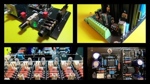
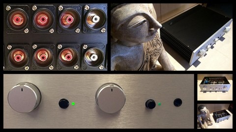
Hifisonix ‘Symphony’ Line Preamplifier

I designed and built this preamplifier while living in Taiwan a few years ago. The Symphony preamp features Baxandall tone controls, up to 7 inputs, a class A 2 W headphone amplifier and a Goldpoint 24 position attenuator. The write-up describes the design process and choices in some detail and my listening impressions:
Part 1 – Ovation Symphony Line Preamplifier V1.0
Part 2 – Ovation Symphony Line Preamplifier V1.0
Specifications_Line and Output Only
Introduction
I have designed and built two preamplifiers over the past few years, this being the third. The first of my recent efforts – after a 25 year layoff – was the X-Altra Mini One, which featured an ultra-simple signal chain based on an LM4562 op-amp. The second was the experimental SCA-1 which was an all-out top of the range IC based design using a TI PGA2320 chip configured in balanced mode, along with LM4562, LME49600 buffers and a headphone amplifier. This design had no tone controls of any sort, but featured a remote control and a 5” GUI TFT display, all controlled by an NXP LPC1768 ARM based mbed controller. I have not got around to housing this design yet – I guess the expense of a large custom case has put me off for the time being. This brings me to the current project, the Ovation ‘Symphony One’. I designed and built a few pre-amps in my early 20’s that featured Baxandall tone controls and headphone outputs, and after reading about Douglas Self’s latest design in Elektor, I was inspired to try my hand again at a full function preamp, incorporating decent (i.e. Baxandall) tone controls, a class A headphone amplifier and an optional MC/MM input board, which would be designed at a later stage. With no pretensions to convenience, this design does not cater for remote control, and has no fancy 5” TFT display like the SCA-1. However, this preamp features the following:-
- The design uses low noise opamps in the main signal path, to achieve outstanding noise performance
- All the op-amps are buffered with discrete class A output stages and their outputs are also bootstrapped at around 600uA into class A mode. The buffers are inside the opamp feedback loop
- All class A operation means the supply lines carry only the fundamental of the output signal and low order harmonics – so no wide band harmonics as is the case with class AB operation, reducing noise and any impact on distortion performance due to magnetic coupling of these higher order components into sensitive circuit nodes; further, with this technique, HF excitation currents are kept off the supply rails, minimizing potential ringing on the supply lines (see Kendall Castor-Perry’s articles on power supply decoupling for example)
- Heavy filtering of the PSU ADJ pin means the wide band noise is about 20 µV, while the additional 22 Ω and 100 µF supply filter on each opamp supply pin reduces HF noise further, and provides tight, localized decoupling for each active amplifier/buffer stage.
- The design uses ‘back terminated’ input signal select switching to deliver very high input ‘offness’
- Strict attention to physically separating the left and right channels keeps channel separation high
- Distortion at 1 V RMS output into 10 kΩ is in the region of 1ppm at 20 kHz, and at 8 V RMS out into 600 Ω better than 5 ppm, again at 20 kHz
- A Baxandall tone control (which can be completely bypassed) offers +-10 dB of boost and attenuation at 100 Hz and 10 kHz with distortion of < 15 ppm at 20 kHz and 10 V peak out
- This preamp features a very high performance headphone output that will drive 32 Ω to >3 V pk-pk and still remain in class A operation at less than 10 ppm distortion at 20 kHz
- 7 input sources and a switchable buffered tape loop
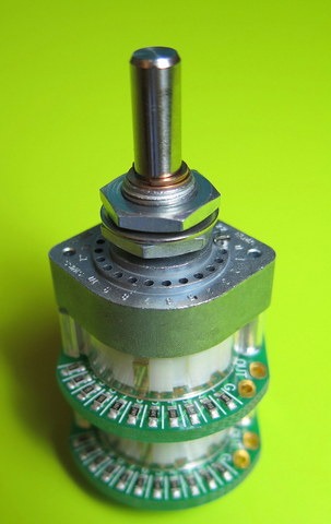
- The volume control is a front panel mount Goldpoint Mini-V 5k log taper unit for the ultimate in transparency and tactile feel

Design Approach: Some General Thoughts
My 2008 X-Altra Mini One preamp is a minimalist design that eschews tone controls and really focuses on doing as little as possible with the source signal, other than providing source selection, volume control and some gain and buffering in order to match the typical 1V required to drive a modern power amp. Input source selection is based on small signal relays (Panasonic AGN series), which, along with a carefully designed power supply and layout, allows this design to achieve about 5 ppm at 20 kHz distortion at 1V RMS into 600 Ω, and <70 ppm at 6.5V RMS into 600 Ω, again at 20 kHz. If applied correctly (and that’s easy to do if you just follow basic, simple layout and circuit design practice) the LME4562 is a wonderful sounding chip. Sloppy layout, bad decoupling and other avoidable design missteps can lead to problems – you are dealing with a device with an OLG of 140dB at LF and a ~55 MHz GBW. In the write up, I comment on the very good sound – open mid-range and top end along with first class imaging. Direct coupling means bass performance is not compromised, and there are no opportunities for electrolytic sonic intrusion, inasmuch as this is a problem with a carefully chosen component.
A year or two later, this was followed up with the Ovation SCA-1. Again, no tone controls, but the volume control and main gain element featured a TI PGA2320 configured in balanced mode, with buffering before and after using LM4562’s and LME4900 unity gain buffers. The PGA2320 has taken quite heavy criticism in some quarters, with claims that they are sub optimal in sonic terms or noisy and so on, but my practical experience is different. You need to feed them from a low source impedance to get the best noise and distortion performance (so something well below 1 k Ω) and the outputs do need to be buffered – although I would say this applies to any op-amp based design that has ‘high end’ pretensions. In the SCA-1, the balanced input signal after the relay selection stage is buffered by a dual LM4562 opamp, which in turn drives each channel of the PGA2320 in balanced mode. The output of the PGA2320 then feeds into an inverting stage and an LM49600 high current buffer, which is inside the opamp’s feedback loop. This configuration will drive a 20 V pk-pk balanced signal into 200 Ω with less than 3 ppm distortion at 20 kHz. At 1V RMS out into 600 Ω, the distortion is a few hundred ppb. A servo keeps output offsets to less than 50 µV. Most of my assessment of the SCA-1 (both subjective and in comparison with the X-Altra Mini, Marantz and various iPods and CD players) has been done with an assortment of headphones including Sennheiser, Audio Technica ATH-900, some Sony IE’s and a very high end Stax tube based system along with some evaluation sessions on the Ovation 250. The design features a very open top end, great bass, imaging and low noise. As further independent evidence to the performance potential of the PGA2320, a 2008 review (and there are more recent iterations of the C-03 that still retain the PGA2320 as the main gain control element) of the top of the line C-03 Esoteric line preamp which uses this chip as the primary gain element and retails at over $10k, gave it top marks for sonics and overall audio performance. In fact, the reviewer claimed it was one of the very best line preamps he had ever heard. And, this was not the only review to similarly rate this Esoteric preamplifier in the top echelon – so did 6 Moons amongst others, and Stereophile also had very positive comments after hearing a system built around one. When thinking about high end audio, one’s component and semiconductor device prejudices are best set aside I have found – whether you believe equipment reviewers or not.
Both of my recent designs (X-Altra Mini and the SCA-1) tell the brutal truth, and especially so with respect to recording quality. But, there is no doubt that the two biggest – by an order of magnitude or more – contributors to sound perception are the recording itself, and the speaker + room interaction. If you have a reasonably large record or CD collection, this can leave you with recordings that lack the right kind of balance given your specific room/speaker setup. Some commentators believe a good speaker will sound good in any environment, and if you think you have a sound problem, then your system is not up to standard. I take the view that in most cases the system is capable of very good performance and it’s the room that’s not always up to the task. I have about 50 CD’s out of 500 that are almost perfect for my listening environment: the bass and treble are well balanced, good imaging, and the overall sound well integrated and pleasing to the ear. This leaves a lot of recordings in my listening environment which need some response balancing and the requirement for a decent tone control, which will be discussed in some detail a little later.

Douglas Self’s two major DIY preamp designs have featured another of Peter Baxandall’s innovations, his Active Volume Control. This approach varies the feedback factor in an active gain stage to achieve a volume control range in the order of 100:1, or about 40dB and it achieves a log like response using standard linear pots which are always easier to get hold of, especially in the 1 k to 20 k range. There are clear advantages to this design, and the fact that the gain need only be as much as is required for ones desired listening level means that it always provides the best signal to noise ratio for a given output level. Some concerns with this configuration are that you have to hang a potentiometer off the sensitive summing node in an opamp feedback network, but the same criticism of course can be levelled at Baxandall’s tone control, or any inverting, current summing circuit for that matter.
Careful layout, screening and the use of quality potentiometers will get a design the rest of the way to decent performance. However, non- summing junction topologies do not suffer from these issues, and any noise appearing between the feedback junction and the amplifier inverting input is amplified by the closed loop gain only, which in a high performance opamp based design, is theoretically a difference of over 100 dB compared to inverting variants. Of course, the issue I raise here applies equally to the Baxandall tone control, where the summing junction is fed from a resistor (from the bass side) and a capacitor (from the treble side). Again, careful layout is required to mitigate any problems. Let me stress, we are talking about noise pick up between the feedback network upper and lower resistors junction and the inverting input of the amplifier element, and not about the inherent noise performance of the inverting or non-inverting configuration.
On the Baxandall active gain stage, the summing junction input impedance at high gain settings can be very low, placing a heavy load on the opamp such that it would be exiting its class A region in the presence of very small output signal levels – just the opposite of what we would intuitively expect. I did some simulations, and the drive current required using a 1 k pot feedback element with maximum gain selected is indeed high at 10 mA. A good opamp (like an LM4562) can easily drive this type of load at 1-2V with single digit ppm distortion levels at 20 kHz; Thus, with say a 10mV output signal in this scenario you could expect 100 ppm distortion. However, I would not consider this a design flaw – maybe at worst an idiosyncrasy of the circuit. Besides, if it is of concern, it is a simple matter to place a class A discrete buffer following the opamp and ensure it is enclosed in the overall feedback loop. Self paralleled opamps in his design to reduce noise and this also solved the drive issue, so his Elektor preamp achieves very low distortion as a result.
A more conventional approach might feed the input signal straight into a potentiometer (sometimes after buffering), placing a gain of circa 5x after this to provide signal level matching to the power amp, which typically would require 1V to drive it to full output power. In this scenario, we are placing a gain stage after the attenuation element, so the amplifier will always be contributing a fixed amount of output noise (ignoring for a minute the current noise contribution which will vary with potentiometer setting). So, at high attenuation factors (so low listening levels), the signal to noise ratio can be severely degraded if the gain element is not carefully chosen. The best signal to noise performance for this type of design is when the volume control pot is set to maximum, so the amplifier noise is masked by the high output signal levels; of course, the source will also probably have a low output Z, so the noise with no signal in is likely to be low in this situation in any event. Most pre-amplifiers use this approach, and with modern gain elements and volume potentiometers typically at about 10 k Ω, the overall subjective performance remains very good. A prime concern usually cited by designers who select this signal chain configuration is to do with overload capability. You can feed in a 2V CD signal into this type of preamp on one of the non-CD inputs (CD inputs are usually attenuated by 20 dB to bring them into line with tuner and recorder output levels which are 200 mV), and by simply adjusting the volume control can prevent any overload. This is how the X-Altra Mini One is configured, and how the attenuation in the PGA2320 is also accomplished (the PGA2320 also offers up to 31 dB of gain which is done by adjusting the feedback factor of the internal opamp gain stage above attenuator settings of +0dB) – this gives an improvement in S/N ratio at low attenuation settings when the opamp is running at unity gain. In my SCA-1 design, the maximum gain as set to 16 dB and the noise levels were extremely low.
However, the third alternative is to amplify the signal first and then attenuate. Further, you can provide a higher input impedance load to the source components, like 47 k or 100 k rather than the 10 k of the input volume control potentiometer, which can be useful if for example you are driving the preamp from a tube based cathode follower where the output impedance may be many k Ω. The output of the amplifier stage can be buffered, biased into class A and thus drive a low value volume control pot, for example 1 or 2 k, which brings with it improvements in noise performance in the follow-on buffer stage. This carries the overload risk, but gets around the noise degradation. But, the overload risk is greatly exaggerated in my view with this type of design. Most digital signal source outputs today (2014) are 2 V, while legacy sources such as tape recorders, analog tuners and so forth, around 200mV. Almost any power amp available on the market will be driven to full output with a single ended 1 V input signal, with some requiring 1.5 V.
This leaves us with two options: attenuate the digital sources by c. 6dB to get the 1V full scale output and amplify the legacy sources by ~14 dB to get 1 V out from 150 mV to 200 mV input full scale. For the Ovation Symphony, I chose the latter course of action, since I will be providing an MM and MC input facility, and possibly a tuner in the future. Further, if you attenuate by 6 dB on the digital source inputs like CD players or music servers and you assume quite reasonable 10k input impedance is required for the pad, this leaves you with a 2.5k source resistance (parallel 5 k resistors with the pot set at the electrical mid-point). You could buffer the digital source first and then drive a low impedance divider, say 2 k for an overall source impedance of 500 Ω, but there is added complexity and the distortion and sonic contribution of an opamp is not zero, whereas good resistors can easily achieve <100 ppb and they don’t require a power supply, decoupling and so on. However, if you go the 20 dB padding route to level all the signal sources to the 150mV ~ 200mV range before boosting them back up by 16 dB to the 1 V required for the power amplifier, then overload can be avoided and you end up with the best of both worlds: Noise is attenuated along with the input signal but unlike the Baxandall active gain stage, there are no potentiometers – with the risk of picking up noise – hanging off a sensitive, 16 dB gain, summing junction. A 10 k 20 dB pad offers a source resistance of ~900 Ω to the 1st stage buffer/amplifier which can get you to the benchmark >110dB SNR ref 1 V out provided the gain device has decent low noise performance.
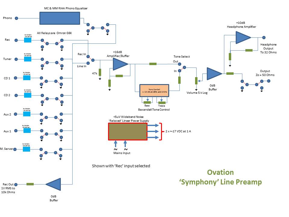
Fig 1 – Ovation Symphony Block Diagram
Ovation Symphony System Level Block diagram (Fig. 1).All of the inputs have jumper selectable -20 dB pads, feeding a low noise 14.4dB gain stage which then drives a 5 k Goldpoint log volume potentiometer. With a nominal 200 mV input signal and the opamp stages running off +-15 V, assuming 12 V pk-pk undistorted output swing, the overload is 20 dB – plenty when the amplifier can be driven to full power at 1V input level. The 20 dB pads are built around a 9 k+1 k divider, so the worst case source impedance seen by the gain stage is about 1000 Ω when selected including the source driving impedance, and when fed directly from a source, much lower than this – you can safely assume on modern equipment 50-100 Ω. There is a small noise penalty to pay for this type of divider arrangement, but in my assessment it does not detract from the overall subjective sound of this pre-amplifier. In the worst case mid resistance setting of the volume control (2.5 k), the parallel combination of the two halves of the potentiometer is ~1.25 k. Since there is no amplification taking place after the potentiometer, only buffering, the noise contribution is very small, and referred to the input, the buffer stage noise contribution is divided by the gain of the preceding stages. Of course, if the tone control is switched in, the noise contribution of the tone control has to be factored in. But, again, because of the way the signal chain is configured, and the use of 5k potentiometers in the tone control section, even with full treble boost, this preamplifier is still incredibly quiet. Further, since for most listening, the volume control will be set between the 9 o’clock and 1 o’clock positions, noise generated by the preceding stages will be attenuated: you get all the benefits of an active volume control with, dare I say, none of the drawbacks.
Small signal relays.I’ve read a lot of commentary on the web about relays in high-end audio applications. There seems to be a fear that after a while they will fail, or the contacts will become corroded or damaged, affecting the signal seriously. Small signal relays like the ones used here are incredibly reliable – after 10 million operations with a load of 10uA, the contact resistance is specified within 10 mΩs of the original 30~65 mΩs of the sample set at the start of the test – the device is specified at 100mΩs contact resistance. The Omron G6K is rated for 100 000 switching operations at full load, and 50 million mechanical operations – i.e. no or very low contact load. Some relays specify potential contact problems if continuously powered up due to outgassing of the plastics and insulation used in the relay. My X-Altra Mini One is never powered down (on 24/7 for months at a time) – I’ve had no problems on the AGN type relays. Another specification that people have concerns with is the minimum rated contact current – a typical spec being 10 µV~10 mV at 10 µA load current where there is a fear or concern that you cannot switch lower levels without affecting the sound. These specs are normally limited by the test gear – not the relay contact performance. Measuring and testing 10 µV~10mV/10 µA contact performance in is no easy task – thermoelectric issues between the contacts under test and the measurement gear for one pose a significant challenge – and trying to do this in a high speed automated test set-up would be expensive. Switches have exactly the same issues and for the most part they are not even sealed. Sealed relays keep atmospheric contaminants away from contacts, and at low signal switching levels, the gold clad contacts stay clean providing consistent contact resistance performance. Let’s also not forget the high frequency performance of small signal relays – they are generally also quite capable of switching RF up to 20 or 30 MHz with minimal loss and therefore qualify as very wide bandwidth devices. A further important benefit of relays is that you can locate the switching close to the signal – long PCB tracks or wires with potential cross talk problems are avoided, as is the case with switches.
For the input source select relays, I used Omron G6K2P series devices. A good reason for their great performance of course has to do with the small physical size, silver with gold clad contacts, and importantly, the fact that they are sealed – so no issues with the ingress of atmospheric contaminants. Another great relay for this type of application is the Panasonic AGN – this is physically smaller, but also features a fully sealed, silver with gold clad contact construction. Neither of these relays is cheap, but they offer a long life and consistent contact performance. In this design, the relays are configured in a ‘back terminated’ arrangement so that the wipers are grounded when an input is not selected, resulting in very high ‘offness’. In conventional arrangements, if you turn the volume fully up with a source playing on a non-selected input, you are likely to just be able to hear bleed through, even on a good layout due to capacitive coupling across and around the contacts – and the problem gets worse as the receiving input impedance gets higher. With the arrangement shown here, there is zero signal bleed through – the technique is very robust in this regard. Of course, for balanced inputs, you will need two relays, rather than the one shown here, so it quickly becomes an expensive proposition. However, in a top end design, which is what I am targeting here, this is not an issue.
The tone control is located on a separate PCB, which also has the headphone socket, mute and tape loop switches. The tone defeat switch allows the tone control to be completely bypassed with the signal routed around the tone block. Note that no switches are used in any of the signal routing duties, including the tone control bypass – this is all done with the Omron relays – the front panel switch simply applies power to the tone bypass relay coil, located on the main board.
The output from the tone select relay feeds the Goldpoint 24 position log law attenuator, and from there it is routed to the output buffer and the headphone amplifier. The output buffer, like the input gain stage and tone control, is also an all class A stage capable of driving 200 Ωs to 10V pk in class A. For the headphone amplifier, I had the choice of going for an LM4990 buffer in an opamp feedback loop as I did on the SCA-1, but this is class AB, and my stated goal was ‘all class A’. The end result is a 2W class A design that features under 10ppm distortion at 3 V output into 32 Ωs, while in class AB it can deliver ~4 W into 32 Ωs.
-
Ovation e-Amp: A 180 Watt Class AB VFA Featuring Ultra Low Distortion

The e-Amp is a 180 Watt RMS (very conservatively rated into 8 Ω ) fully balanced symmetrical (‘FBS’) amplifier featuring an emitter follower triple (EFT) bipolar output stage and beta enhanced VAS stage.
The amplifier can be configured using jumpers for TMC (Transitional Miller Compensation) or straight Miller compensation (MC). The VAS can be lightly loaded to reduce the overall loop gain, but increase the open loop -3 dB bandwidth to 40 kHz also using a jumper. I have called this compensation option ‘Wide Band’ or WB. This allows four compensation schemes to be selected – MC, TMC, WB-MC and WB-TMC. With the e-Amp, by simply inserting or removing a few jumpers it can be flipped from one compensation design another – how it is ultimately tuned, and how it sounds, is up to personal choice.
A microprocessor based protection board takes care of transformer in-rush current limiting at power-up, speaker muting (unusually, using low Rds(on) Trench mosfets), over temperature, DC offsets and output short current protection.
Subjectively the e-Amp produces great imaging, a very smooth, open mid and top end with plenty of bass depth and slam. I personally doubt you could ask for anything more from a power amplifier.
I hope you enjoy reading about the Ovation e-Amp as much as I enjoyed designing, constructing and writing about it.
Here is a .pdf copy of the e-Amp article giving a detailed circuit description with a design discussion covering topology, device technology selection and compensation design (circa 60 pages and 10MB)
__________________________________________________________________________________________________________________________________________

1.0 The e-Amp: A Design Discussion
________________________________________________________________________________________________________________

Although the relationships between key circuit performance parameters are well understood, there is no universal approach or methodology to designing audio amplifiers. You either get taught in engineering school how do it in very general terms, you stick with it and adapt it over time, or you work out your own methodology. Of course, there are now some very good books on the specific subject as well. I use LTSpice very extensively in the design process, since even though you can calculate the required component values to quickly arrive at the initial 1st round nominal values, there is a lot of fine tuning required to get a really good, high-performance design, and that’s even before we start to think about the critical PCB layout and wiring issues. To be sure, what is seen in the circuit model on a computer does not always reflect what is measured or observed on the prototype in the detail, but its close enough to help understand what’s going on in the prototype, and to make sensible tweaks. A major reason for the discrepancy is to do with the accuracy of the models in the simulator to prototype direction, but there are also problems going from the prototype to the model because the prototype real world components with parametric spreads and parasitics (e.g. capacitors, trace inductances and so on) result in behaviour you don’t see at first on your computer, and a typical example is the behaviour of EF triples and cascodes in the presence of PCB trace inductance. Further, there are a few cases where modelling and simulation are problematic, a good example being the FBS topology with mirror loaded LTP (to be discussed a bit further on), which simulates perfectly, but is not DC stable in the real world, rendering it useless in a practical amplifier without some form of VAS DC common mode current control circuit.

1.1 e-Amp Topology: ‘Fully Balanced Symmetrical’ (FBS)
The choice facing the designer of any power voltage feedback amplifier is to go with either a Lin (so called because it was HC Lin of Bell Labs who first proposed the topology in the 1950’s) or FBS topology or some derivative (and there are many) of either. Like the feedback debate, there are those that swear by the Lin topology (popularized by Douglas Self who used it as the demonstrator of his now famous ‘blameless’ amplifier concept) and others that say the FBS can do no wrong. The criticisms from some quarters leveled at the Lin topology stem from the fact that the VAS is not symmetrical and therefore the drive to the output stage is not symmetrical since you have a buffered common emitter stage usually loaded with a current source. The common emitter VAS amplifier can provide substantial currents into the output stage, but the current source limits the drive on the other half of the waveform. As a result, the slew rate (SR) is also not symmetrical, and when Self’s efforts to mitigate this problem are studied, one quickly concludes it is a hopeless cause. Balanced designs suffer none of these drawbacks, offer an additional 6 dB of loop gain, and neatly cancel 2nd harmonic distortion, although some practitioners don’t like this, citing the resultant missing, or lower level, even order harmonic distortion spectra as a negative influence on amplifier sound. There are well known techniques to convert a standard single ended LTP to a balanced drive VAS in which the drive and slew rates are symmetrical. The earliest single ended LTP input to balanced drive VAS I have been able to identify was in Bart Locanthi’s design from 1966 while he was at JBL. Subsequently this was used to good effect by a number of manufacturers, and popularized by Hitachi Semiconductor in their mosfet applications data handbook from the very early 1980s, but I don’t know if they got it from Locanthi, or if it was developed independently. Robert Cordell used a standard single ended LTP to balanced VAS stage topology in his amplifier with mosfet output and error correction, also from the early 1980s. In the FBS topology, originally developed by John Curl, and his subsequent derivative utilizing a folded cascode, SR’s and drive to the output stage is symmetrical and VAS output current drive capability is substantial. However, the FBS small signal stages are generally more complex, and compared to the Lin topology, there is a $ cost penalty (albeit small) and the PCB layout also takes a bit more effort. The Lin topology is simpler, lower cost and still achieves remarkably good results as evidenced by Self’s work. In terms of output stage drive capability, if one uses an EF3 or CFP output stage, the drive issues with the Lin can be reduced substantially, though you cannot readily overcome the differences in positive and negative SR’s. Given some of the shortcomings of the Lin, and I have to say my positive experience with the FBS topology in the Ovation 250 amplifier, the FBS was also selected for the e-Amp. The penalty is slightly higher cost and complexity for the small signal components (maybe around $4 on a one off like this), but I think for a high performance amplifier this is a small price to pay for symmetrical drive of the output stage and an additional 6 dB of open loop gain. I would add at this point that if designing an amplifier for high volume commercial applications, the Lin topology would be my first choice because of its simplicity and cost effectiveness. But, like the Ovation 250, the Ovation e-Amp has definitely not been designed to a price point.

The Ovation e-Amp 1.2 Front End Design
A general discussion about input device technology, Re, SR, Input Overload, Tail Current and Input Filter
JFETs or Bipolar?
Solid state amplifier designers have a choice of 2 basic device technologies for the input stage: bipolar or JFET. Some idiosyncratic designs use mosfets, but I will not cover these here. The gm of JFETs is much lower than un-degenerated bipolar devices, and in VFAs using conventional Cdom compensation, this translates into higher slew rates for a given distortion mechanisms. JFETs can offer improved RFI immunity over un-degenerated bipolar devices, and some designers claim they are more linear than bipolar devices, but this has been contested. They are unmatched in applications requiring high input resistance (great for condenser mic preamps or photo-diode amplifiers for example) and their very low noise current makes them ideal for things like MM cartridges, or any other high impedance sources. These are all very strong points in favour of the JFET. John Curl, the designer of Parasound amplifiers, carved out a name for himself as the foremost proponent of JFET front ends in audio power amplifiers. Nelson Pass, a class A, ultra simple signal path exponent is also a JFET fan, as is Charles Hansen of Ayre. However, JFETs are not without their problems. Firstly, in FBS topology designs, quite some effort is required to match Idss and Vgs vs Id characteristics to minimize distortion and DC offsets. In both JFET and bipolar designs, balance between the LTP two halves is critical for lowest distortion – however matching JFETs is much more difficult because the device parameters are somewhat ‘looser’ than bipolar devices. Discrete designs using this approach will require a servo to correct for both initial offset and temperature drift. Input capacitance in JFETs is high and very non-linear with respect to the gate drain voltage, causing distortion. One way of getting around this is to cascode the diff amp devices so that Vds is fixed. In bipolar designs the front end LTP stages are often cascoded (as is the case with this design) so that small signal, high hFE devices can be used, since high voltage high hFE transistors are not readily available. Cascoding bipolar devices also aids in PSRR and improves linearity by mitigating Cob effects. In JFETs, the lower gm also translates into lower overall open loop gain, if this is an important design goal (some designers prefer lower loop gain), the lower inherent gm is not a problem, but a virtue.
Modern bipolar input power amplifier designs are almost never configured without input stage degeneration – this in order to improve slew rates and avoid the now extremely well understood TIM mechanism. This also immediately mitigates RFI ingress (an objection often raised by designers who prefer JFETs) but the penalty is additional noise contribution from the degeneration resistors – however the levels are low enough so that they are of no concern in a power amplifier. Of course, gm is also lowered, but the designer has a bit more flexibility as to how much. The input capacitance in bipolar devices is lower, and when the degeneration is factored in, linearity easily matches or exceeds JFETs. Input bias currents are of course higher, and if the tail current is high (which is what I tend to do in my designs to enable high SR’s with standard MC), the feedback and bias resistors need to be low to minimize any resultant offset. However, high input capacitances in JFET designs also mean there is a practical upper limit to the feedback resistor values in those designs as well, to say nothing of the noise contribution. Bipolar input stages are much more DC stable than JFET discrete stages – typically on a well designed power amp using high beta devices 10 ~ 15 mV of offset without hFE matching, and temperature drift of under 10 µV/C. This allows the feedback network to be capacitively coupled (more on this point later), and a simple pot adjustment for offset voltage suffices. Unlike JFETs, good small signal bipolar devices are ubiquitous, and devices from the same batch are remarkably well matched – Vbe of <;2 mV and hFE to within 20% is quite typical. Tighter matching by hand is therefore an absolute cinch, and on BC547C/557C you can easily match devices from the same batch to within 2 ~ 3% at hFE = 500+. The golden age of the JFET is long passed, and some of the best devices ever developed for audio (especially Toshiba) have been EOLed (End Of Life – semiconductor industry parlance for end of production and no longer available). There is quite some niche JFET industry in audio sourcing NOS, faking devices and generating ‘vapor ware’ – i.e. promises of matching N and P channel JFETs on roadmaps that never materialize. No doubt, the very fact that these devices are no longer in production has driven up prices and allowed all sorts of magical audio properties to be attributed to them . . .
There are as many bipolar front end solid state amplifiers in the Stereophile ‘A’ grade category as JFET and Tube designs. Clearly, overall execution and technical expertise enables designers to avoid the cons and exploit the pros of their chosen devices to deliver top class results. For all of the reasons outlined above, and like the Ovation 250 design, the Ovation e-Amp also uses an all bipolar front end.
Slew Rate, Tail Current, Front End Overload and Input Filter
In order to avoid TIM, Leach describes succinctly the requirements to ensure that the input overload capability is not exceeded. The input stage must remain operating in its linear region with the maximum expected input signal dynamic both in terms of magnitude and rise/fall time. Linked to this, the LTP tail current must be able to charge and discharge Cdom quickly enough to ensure that the peak differential voltage between the non-inverting and inverting inputs to the amplifier do not exceed the maximum linear operating region of the input stage. If either of these two conditions is not met, TIM can occur.

Fig 1 – LTP Model Fig. 1 shows the model I used to check for input stage overload capability. The tail currents, I1 and I2 along with the value of Re determine the max input voltage input the stage can handle whilst still remaining linear. Because of the resistively loaded LTP’s (and use of Cdom or TMC compensation), I like to run my front end diff amps stage ‘rich’ with a tail current of about 10 mA (so 5 mA per side) and Re at about 100 Ω as this meets a nominal 0.5 V maximum input signal capability while still keeping the loop gain reasonably high. Because the LTP is resistively loaded, under worst case slew conditions when either Q10 or Q13 are turned on hard and providing the maximum amount of current into Cdom (C10 and C11), a large portion of the tail current is still shunted away from charging Cdom through R71 and R72. In mirror loaded LTP’s, all of the tail current under these circumstances is diverted into charging Cdom, so for the same slew rate, you can get away with half the tail current. The second important reason for running the tail current high, as in the Ovation e-Amp front-end configuration, is in order to achieve high slew rates using standard MC. This translates directly into modest input filter requirements (-3 dB circa 350 kHz) which would otherwise have to be set at a much lower cutoff frequency to ensure there would be no transient overload on the input stage. Due to the compensation design on the e-Amp (to be covered more fully later), a low value for Cdom is used (effectively 25 pF), which results in a slew rate of ~ 155 V/ µs (front end filter disabled). This high slew rate is as a direct result of the high tail current and heavy front end degeneration. Fig 2 shows the output of the model where the input voltage is plotted against the LTP collector currents. The linear range is about ±0.6 V. For higher values of Rem and/or tail current, the input linear operating range increases, but this has to be paid for with a reduction in gm.
;

Fig 2 – Bipolar LTP Linearity with Degeneration If this difference voltage exceeds the linear input operating voltage as shown in Fig. 2 (which is just under ±0.6 V), the amplifier cannot be guaranteed free of TIM distortion. Fig. 3 plots the error signal as the delta between the non-inverting input and the inverting input. To simulate this error plot, I fed in a square wave of 25 kHz at ± 1 V pk-pk with a rise time of 100 ns. This is an implausibly fast rise and fall time, but clearly shows the absolute limits of the front end overload capability. If the input stage saturates, there is no feedback – the amplifier is running open loop until the loop recovers. As a result, the output it is likely to end up stuck at one of the supply rails until the loop can gain control again – a very messy situation indeed. However, the cure is simple – either lower the input filter cut off frequency and/or reduce the input stage gm by increasing Re until the difference voltage falls below the maximum linear operating range per Fig. 2.
The front end design and value selected for Cdom therefore ensures that the e-Amp will never run into TIM. Fig. 3 shows the result with no input filter (capacitor value set to 0 pF) and the peak error signal (red trace) is >; 1.5 V. With the Input filter -3 dB cut-off set to 720 kHz, the peak error signal is the lower red trace at about 0.8 peak, while with a 2 µs rise/fall time signal (far more realistic), the peak error signal is 0.3 V – well within the overload capability of the front end. Connecting each channel of a wideband dual channel scope to the inverting and non-inverting input and subtracting the two will directly display the difference waveform and something very similar to that which can be seen in Fig 6. Use a fast rise time square wave input signal for this test – 100 ns is about right – with the front-end filter in situ.
;

Fig 3 – e-Amp Input Stage Overload Capability In the final design, I lowered the input -3 dB cut off frequency to circa 350 kHz (R68 and C24) as a precaution against RF ingress.
The front end design goals can be summarized as follows:-
1. Ensure that under absolute maximum input drive conditions (i.e., just prior to clipping) the input stage remains linear, as shown in Fig 2 and Fig 3. Use 2 µs rise/fall times for this design step. Increase RE and/or the LTP tail current to ensure this condition is met. Do not provide any more headroom on the front end stage than is necessary, since this has to be paid for by a reduction in loop gain and ultimately, increased distortion.
2. For conventionally Miller Compensated configurations like the e-Amp, run the LTP current high (so 5 ~ 10 mA) in resistively loaded designs to ensure high slew rates and sufficient current to charge and discharge Cdom whilst at the same time providing the current demanded by the LTP collector load resistors.
3. With regard to the input filter, adjust the cut off frequency on the final prototype by looking at the output into an 8 Ω load, and making sure there is no overshoot, being careful not to be too aggressive. An input filter -3 dB of between 300 and 500 kHz is about right for design like the e-Amp. For this design step, use a fast rise time of about 100 ns.
4. Cdom, Re, tail current and the input filter are selected based on a set of tradeoff’s which in turn are highly dependent upon output device Ft.
1.3 LTP Current Source
I spent some time deciding whether to go for active current sources or to use the legacy technique (Marshal Leach and Bart Locanthi designs are good examples) which is to derive the LTP tail currents from a Zener + resistor reference. For the active current sources, one can use the classic transistor+ diode reference, the two back-to-back transistor variant or even a current mirror, where the attraction is that a single resistor can set both +ve and –ve tail currents, albeit with some additional complexity over the other options.

Fig 4 – LTP Current Source Options 
Fig 5- Current Source Positive Supply Rejection ;
Figure 4 details the options looked at and from left to right they are an ideal theoretical current source with infinite output impedance (for reference), the standard Vref based current source, the popular two transistor type and finally, the Zener derived source. On the output side of the LTP’s (i.e. the diff amp collector load resistors) all of the current sources perform well in terms of +ve supply rejection (see Fig. 5). However, the Zener reference rejection is a little worse at lower frequencies at -147 dB vs 154 dB for the active types and the theoretically perfect current source. The major limitation of the +ve supply rejection is due to the coupling of the +ve rail noise signal through to the bases of the LTP transistors via Cob. Here we see that one of the benefits of cascoding the LTP transistors is to reduce this effect and improve PSRR, although at -126 dB there may be a temptation to concede that it is good enough without it.
Fig. 6 details the –ve rail rejection performance. The green trace is the ideal theoretical current source which is the reference. In both the active types, -ve rail rejection performance falls off (i.e. stops improving) between about 10 Hz and 200 Hz, whilst the Zener derived reference only levels off at 20 kHz and remains considerably better than the other practical options right up to the simulated limit of 10MHz. On the active types, you can cascode the current source transistor, or use a three transistor variant, to get better performance, but the Zener reference performance still cannot be matched.
;

Fig 6 – Current Source -ve Rail Rejection Performance ;
In Figure 6 above the green trace is the reference based on an ideal current source, dark blue and red the active current sources, and the light blue trace is the Zener + resistor source.
On the e-Amp I ended up going with the two transistor variant (3rd from left in Fig 4) – its performance is on par with the other active designs, its well tried and tested. The Zener reference offers advantages at HF that are clearly evident from the simulation above, but you then have to worry about matching the diodes, and using some big decoupling and filtering capacitors. During prototype development, I consistently got readings across the 1% current sense resistors (R44 and R47 in the e-Amp circuit diagram) of within 2 mV of each other – a 0.6% current source match withoutany selection. This is considerably better than any of the other current source options.
1.4 LTP Load Options
For good performance, the tail current must be shared equally between the two transistors in each LTP (same applies to single ended designs as well). Simulation shows that only a small imbalance can lead to appreciable distortion. Traditionally, audio power amplifier designers have used either resistive load or a current mirror. With a current mirror, you get very good balancing between the transistors in the LTP pair and very high gain. Additionally, as discussed in section 1.2, the SR is doubled over that of resistive loading because all of the input stage tail current can be steered to charge Cdom – none of it is wasted flowing into the collector resistive load. On the face of it, a current mirror load looks like a great solution – and it is on single ended designs like the Lin. However, in the FBS topology, current mirror LTP loads are not DC stable and the amplifier output drifts towards one of the supply rails and remains locked up there – a conventional DC servo won’t help either – and as a result, you have to add a common mode current loop (CMCL) balancing circuit to keep the amplifier output centered.
Further complications with the mirror load are that the amplifier loop gain is much higher and the designer has to wrestle with additional work on amplifier recovery after overload (clipping).
The resistive load LTP was chosen for the e-Amp:- it is simple, there are no DC balance issues, ‘sticky rail’ occurs only in the VAS stage and as we will see a bit later, is easily remedied – and distortion performance is still outstanding. Regarding the requirement to balance tail current, this is set by the input voltage required by the VAS buffer and VAS output transistor Vbe’s plus the voltage drop across the VAS emitter degeneration resistor. The easiest way to do this in practice is to calculate the initial resistor value, check it on a simulator and then tweak the final LTP collector load resistor on the prototype for lowest distortion. The process is simply to take 2 Vbe (since the VAS uses a two transistor follower configuration), allow for a further circa 1 ~ 1.5 V drop across the VAS amplifier emitter degeneration resistor (this is R27 and R69 in the e-Amp circuit diagram) giving around 3 V. The load resistor is then calculated based on 0.5 x the LTP tail current which is 5 mA. In the e-Amp this gives a collector load resistor value of 680 Ω. In the final design, I checked the value to ensure good balance and thus lowest distortion. This value will repeatedly give the lowest distortion across any number of amplifier replicas. Of course, a mirror load with well matched transistors will give better amplifier to amplifier LTP current balancing, but this comes at the expense of the CM balance issues discussed above. Separately, the other aspect investigated on the e-Amp was the effect of unbalanced currents between the two LTPs. Differences of up to 5% have only a minute effect on distortion – in the order of 2 ~ 3ppm. It is the balance between each half of the individual LTPs that is critical for low distortion, and this of course applies to both single ended and FBS topologies
1.5 LTP Load Options
For good performance, the tail current must be shared equally between the two transistors in each LTP (same applies to single ended designs as well). Simulation shows that only a small imbalance can lead to appreciable distortion. Traditionally, audio power amplifier designers have used either resistive load or a current mirror. With a current mirror, you get very good balancing between the transistors in the LTP pair and very high gain. Additionally, as discussed in section 7.2, the SR is doubled over that of resistive loading because all of the input stage tail current can be steered to charge Cdom – none of it is wasted flowing into the collector resistive load (see OR and OR in Fig 10). On the face of it, a current mirror load looks like a great solution – and it is on single ended designs like the Lin. However, in the FBS topology, current mirror LTP loads are not DC stable and the amplifier output drifts towards one of the supply rails and remains locked up there – a conventional DC servo won’t help either – and as a result, you have to add a common mode current loop (CMCL) balancing circuit to keep the amplifier output centered.
Further complications with the mirror load are that the amplifier loop gain is much higher and the designer has to wrestle with additional work on amplifier recovery after overload (clipping).
The resistive load LTP was chosen for the e-Amp:- it is simple, there are no DC balance issues, ‘sticky rail’ occurs only in the VAS stage and as we will see a bit later, is easily remedied – and distortion performance is still outstanding. Regarding the requirement to balance tail current, this is set by the input voltage required by the VAS buffer and VAS output transistor Vbe’s plus the voltage drop across the VAS emitter degeneration resistor. The easiest way to do this in practice is to calculate the initial resistor value, check it on a simulator and then tweak the final LTP collector load resistor on the prototype for lowest distortion. The process is simply to take 2 Vbe (since the VAS uses a two transistor follower configuration), allow for a further circa 1 ~ 1.5 V drop across the VAS amplifier emitter degeneration resistor (this is R27 and R69 in the circuit diagram) giving around 3 V. The load resistor is then calculated based on 0.5 x the LTP tail current which is 5 mA. In the e-Amp this gives a collector load resistor value of 680 Ω. In the final design, I checked the value to ensure good balance and thus lowest distortion. This value will repeatedly give the lowest distortion across any number of amplifier replicas. Of course, a mirror load with well matched transistors will give better amplifier to amplifier LTP current balancing, but this comes at the expense of the CM balance issues discussed above. Separately, the other aspect investigated on the e-Amp was the effect of unbalanced currents between the two LTPs. Differences of up to 5% have only a minute effect on distortion – in the order of 2 ~ 3ppm. It is the balance between each half of the individual LTPs that is critical for low distortion, and this of course applies to both single ended and FBS topologies.
1.6 Feedback Network Coupling
There is a lot of commentary on the web (and in books) about the impact of electrolytic capacitors on amplifier sound and feedback network capacitive coupling. When you pass an audio signal through a suitably sized, quality electrolytic, the AP distortion analyzer shows zero (0) distortion – which, as Self points out in ‘Small Signal Analog Design’ intuitively it should do because it is a short at AC. DA and DF are usually put forward as having detrimental sonic impact, but no concrete evidence to this effect has been shown. The usual solution to get around using an electrolytic capacitor is to use an opamp based servo. However, servo’s are not without their problems, and one has to question whether or not the additional complexity really does bring real sonic benefits. Cordell has pointed out that servos are inside the amplifier feedback loop (as is the coupling cap), and this could also impart a sonic signature. Further, under overload conditions (severe clipping), or situations where there is a lot of very low frequency program material, servos can misbehave, and some sort of DC offset protection is needed for back-up. For this design, I capacitively coupled the feedback network using C7 and C23 to the inverting input of the amplifier. C7 is a large 1000 µF 16 V electrolytic device which is deliberately oversized in order to get around low frequency electrolytic distortion – a problem Cyril Bateman documented in the 1980’s. Provided you keep the AC voltage across an electrolytic below 40 or 50mV, this form of distortion can be eliminated. At HF (so ~ 1 MHz and above), the construction and lead inductance of electrolytic capacitors can cause impedance peaking, which will cause a dip in gain, and this is addressed by C23, a 0.1 µF poly capacitor which simply bypasses the electrolytic. The input transistors are matched for hfe to within 10% and this gave offsets of <;5 mV in two prototypes and in the two final boards. This design does not use a servo and therefore provides output offset adjustment facility by means of R80. Offset drift due to shifts in temperature from c. 25 ℃ to 65 ℃ is less than 1 mV and therefore well below any level that need be of concern.
1.7 The VAS (or more correctly, the TIS or Trans Impedance Stage)
In a conventional Miller Compensated (MC) voltage feedback amplifier, the VAS is in the form of an integrator, with the integrator capacitor formed by Cdom, and the input current provided from the LTP stage collector current. In the closed loop condition, the VAS stage thus has a critical task in converting what is a small signal current of a few micro amps (closed loop condition with normal program material) into a voltage that may swing 100 Vpk-pk or more on a reasonably high power amplifier.
Critical design goals for any VFA VAS can be summarized as follows:-
- Convert small input currents from the front end LTP stage into large output voltages – this is therefore a high gain stage
- Highly linear – closed loop input LTP and VAS distortion should be in low single digit ppm range
- Provide adequate current drive to the output stages – the VAS standing current should therefore be much higher than the expected typical drive current to the output stages, including the usual buffer under worst-case conditions. It goes without saying then that this must be operated well into the class A region under allload conditions
- Swing to within a few volts of the supply rails ideally – so, maximize the potential power from the supply rails
- No ‘rail sticking’ – come out of clipping cleanly and with no parasitics
- Be tolerant of supply rail noise
For a VFA, there are many VAS variants but I will stick to conventional options which are the common emitter, Hawksford, cascode and folded cascode. It is important that the VAS local loop gain (i.e. the amplification stage enclosed by Cdom) is high in order to ensure maximum linearity and for this reason the VAS (Q29 and Q30 in the e-Amp circuit diagram) transistors are preceded by ‘beta enhancement’ transistors Q8 and Q16. Without these transistors, the LF open loop gain (when the amp is configured for conventional Miller compensation) is reduced by about 12 dB (from 83 dB to 71 dB), and this has an important impact on the distortion performance of the amplifier across all frequencies.
") Figure 7 – Conventional Beta Enhanced VAS
Figure 7 – Conventional Beta Enhanced VASThe collector output of the VAS can either drive the Vbe multiplier directly or use some form of cascode. Cascoding (See Fig 10) is usually used to enable the use of low voltage, high hfe small signal transistors for the VAS amplifier. Cascoding also increases the local VAS loop gain. It is very important that the VAS amplifier transistor, or if a cascode is being used the cascode transistor, has low Cob – and this means in the 2 pF to 3 pF region. The base collector voltage modulates Cob as it swings with the applied input signal, and this is a significant source of distortion in the VAS. Cascode transistors are typically biased at about 3 ~ 5 volts off their associated rails as shown in Fig 7. In general, the approach shown in Fig 7 is sufficient (20 ppm ~ 30 ppm open loop distortion at 20 kHz) although the Fig 9 variant will show about half that due to the reduction of Early effect in Q19.

Fig 8 – Hawksford VAS Another interesting VAS design, is the Hawksford Cascode shown in Fig 8, which achieves reductions in stage distortion an order of magnitude lower than conventional designs whether cascoded or not. In the Hawksford cascode, the cascode base current (an error term) is cancelled by drawing the base current through the emitter degeneration resistor (R27 in Fig 8) and returning it to the collector current of the same transistor (also known as ‘re-circulating’).

Fig 9 – Cascoded VAS Stage ;
In the Ovation e-Amp, I chose to use a conventional VAS structure as shown in Fig 7. Since no cascoding is involved, the output voltage swing is maximized – no auxiliary boost supply is required for the front end which is often required with cascode VAS stages (and often seen on mosfet amplifiers to meet the higher Vgs threshold). In simulation, the e-Amp VAS stage + pre-driver will swing 200 Ω load to 100 Vpk to pk at 20 kHz with less than 0.2% distortion, and with a load of 10 k, the figure is in the region of 6 ppm. Given the simplicity, this is good performance indeed.
Due to the high LTP current of 10 mA, when the e-Amp VAS transistor is driven into saturation, there is significant base charge storage in the main VAS transistors, which manifests itself as 3 ~ 4 µs of overhang or ‘stickiness’ on both the positive and negative peaks. At 20 kHz, this results in a truly horrible looking output waveform (see Fig 10 below) and a rapid and dangerous increase in amplifier supply current. The cure here is to use a Baker clamp which shunts base current away from the VAS transistor under overdrive conditions. I used BAV21 diodes (D10 and D11 in Fig. 1) because of their fast switching (c. 50 ns), and very importantly, reverse bias capacitance, which is typically in the region of about 1.2 pF at low reverse voltages. As a result, the Ovation e-Amp comes out of clipping very cleanly and there is little distortion contribution from the modulation of the diode reverse capacitance with VAS output voltage – in the region of low single digit ppm and swamped by other mechanisms in a practical amplifier such as this.
In designs driving mosfet output stages which have high input capacitance, rail sticking exacerbates local parasitic ringing in of the VAS as it exits clipping. This is caused by dynamic short term changes in device parameters (VAS and the mosfets input capacitance) with the changing signal voltage. The amplifier feedback loop tries to correct for this and the result is ringing. Focusing on trying to fix this problem with loop compensation will not work. In all cases, a decent VAS transistor (avoid MJE340/350 types for example) and a Baker clamp will clean things up. Bottom line: sticky rail has to be avoided at all costs.
;


;
;
;
;
;
;
;
;
Figure 10 – ‘Sticky’ Rail – Waveforms Without Baker Clamp (L) and with Baker Clamp (R). Waveforms captured at emitter of the driver stage. Vertical Scale is 50 V/division.
Some designs (e.g. John Curl’s HCA-3500) and the earlier Krell amplifiers used mosfets configured in common source or folded cascode in the VAS stage. These designs will typically not suffer from rail sticking (the base charge storage mechanism in mosfets is different to bipolar devices and related to gate capacitance), and the saturation voltage is very low allowing the full rail of the amplifier to be exploited. Further, the front-end stage can be run at a higher gain (ratio of Rdegen to LTP collector load resistor) because the threshold voltage of the mosfets is higher than bipolars, allowing the use of a higher value LTP load resistor. However, the input capacitance of mosfets is both high and very non-linear; for this reason, it makes more sense to use MIC with these topologies and not MC. Additionally the PSRR in folded cascode designs is not as good as the common source variant, so these designs also benefit from capacitance multiplier techniques in the small signal and VAS supply rails. For now, this probably a topology I will reserve for further investigation in the future.
1.8 Keeping Things Quiet – Ripple EaterThe e-Amp employs ripple eater circuits (Q1, Q2, and associated components) to remove rail noise. Although the front-end current sources are heavily filtered and the LTPs are cascoded, if you are really looking for the best possible noise performance, a ripple eater is an invaluable circuit technique. The photo below (Fig 11) shows the supply rail noise at 150 W into 8 Ω and – the upper trace is the mains ripple measured at V+ and superimposed on that the output signal. The bottom trace shows the noise on the supply rails to the front end after the ripple eater and it is well over 30 dB down. When this is coupled to the supply rail rejection afforded by the LTP pairs (through the action of feedback), hum and noise performance is very good – total wideband noise measured at the output is well under 1 mV into 8 Ω.
Note also that the output signal appears as a half wave rectified replica on the supply rails. When playing music, the rails are ‘loaded’ with wideband hash from the rectified output signal (fundamental and harmonics to many hundreds of kHz) and this can feed into the front end and affect performance – and especially so at higher frequencies. Cascoding helps by preventing HF feed through via the collector base capacitance of the LTP pairs, and the e-Amp of course uses both techniques.

Figure 11 – e-Amp Ripple Eater performance
1.8 Output Stage
Mosfets (lateral and vertical types) have some very useful properties, chief amongst them are the lower drive requirements at audio frequencies and lack of secondary breakdown – simple current limiting is ample. Lateral mosfets are much more rugged than bipolar devices and can handle higher peak currents. Mosfets have a much higher Ft than bipolar devices (300 MHz is quite common), so compensation can be easier while more feedback can be applied if that is your persuasion, although you still have to look out for parasitic output stage instability – the solution is the same as for bipolar devices: use a gate stopper (=base stopper for bipolar) but the value is usually about 10x to 20x higher at 30 ~ 100 Ω. Simple buffering of the VAS is all that is required – usually no need for a double or triple follower. But, mosfets need to be reasonably matched if multiple pairs are going to be used in a linear application like a power amplifier. Thermal stability on lateral types is also good, however it usually comes at the expense of quite high drain current (to achieve the zero TC bias point) compared to bipolars.
Self showed that in mosfet output stages, the gm variation in the cross over region is substantially worse than in bipolar designs, and it is very difficult to get anything remotely like smooth signal handoff across the two halves of the output stage – a trick bipolar output stages are much better at. That said, Cordell and a few other designers have made the case that Self’s mosfet models are inaccurate, and the gm cross over discontinuities nothing like as bad in the real world. However, if you want to reduce the cross over non-linearities to manageable levels, then the output quiescent current has to be set quite high – typically 120 mA to 150 mA per pair, and I have seen figures of 200 mA in some designs. On a big amplifier, this might entail 4 pairs totaling out at 600 mA to 800 mA on ± 65 V rails: – thus, you already have an output stage standing dissipation of 78 W to 104 W. This is about twice as much as an equivalent 4 pair bipolar output stage with 0.33 Ω output emitter degeneration resistors, although some designers would argue you may be able to get away with just 3 pairs of mosfets for the same rated power, which is a point I might concede.
Hawksford’s seminal output stage error correction circuit (HEC) addressed mosfet output stage non-linearity, with an early practical demonstration by Robert Cordell. Using this technique, he demonstrated a mosfet amplifier that surpassed bipolar output stage designs in performance terms. More recently, the ‘Pretty Good Poweramp’ or PGP, designed by Edmond Stuart and Ovidiu Popa used HEC and an advanced mirror loaded FBS front end design using nested feedback techniques to demonstrate full power 20 kHz THD of under 1ppm into 8 Ω.
Bipolar devices are easy to apply (although they need VI protection, or very generously designed output stages) and are currently about 30% ~ 40% less expensive per pair. However, for a high quality amp, you do have to factor in the additional driver stage and protection costs, and this means that output stage costs at a systems level probably favour mosfets. If the emitter degeneration resistor on bipolar designs is a reasonable value e.g. 0.27 to 0.33 Ω, matching of output devices, other than ensuring that they are from the same tube, is not required for good current sharing and distortion performance. On two Ovation e-Amp prototypes, I measured a worst case spread across pairs of emitter degeneration resistors of 6 mA and 4 mA – i.e. under 8%. It should noted in the design presented here that the output emitter degeneration resistors are not matched and are 5% types. Modern high power 200 W 15 A bipolar devices have Ft’s up at 30 MHz. While this is not as good as mosfets, it nevertheless facilitates designs with respectable amounts of feedback at 20 kHz – far removed from the days when power device Ft’s were in the order of 2 MHz. Since the hard turn on threshold voltage of bipolar devices is about 3 ~ 4 times lower than mosfets (0.65 V vs. 2 to 2.5 V), higher supply rails to the driver and VAS stages are not required in order to maximize the output device supply rail power delivery. The disadvantages of course are a more complex drive circuit.
The better open loop linearity – a correctly biased EF3 typically produces about 0.1% open loop distortion at mid power loads, rising to about 0.8% at full power – lower output stage quiescent current requirements in Class AB, and easier matching requirements were the reasons I chose to go with a bipolar output stage.
The output stage configuration used is a ‘triple follower’ based on the Locanthi ‘T’ circuit, developed in the 1960’s by Bart Locanthi. It was, and remains, the breakthrough bipolar amplifier output stage configuration and still the best choice if you are looking to maximize the gain bandwidth of a class AB output stage. Like the CFP output configuration however, you still have to take care of emitter follower parasitic oscillation. Topologies like the CFP or Darlington, might respectively give a bit more output swing, or load the VAS a little less, but the ‘T’ is the best overall solution where supply rail voltages are not a restriction, which is the case in the Ovation e-Amp.
For the ‘T’ the designer can employ either an EF2 (i.e. two transistor emitter follower) or an EF3 (three transistor emitter follower, also sometimes just called a ‘triple’ or EFT). I did some Spice simulations that showed that a triple has about an order of magnitude lower distortion in a closed loop amplifier compared to the double. Furthermore, insofar as distortion is concerned, the double shows little tolerance for changes in output load – just the kind of thing to be expected when driving a speaker where the impedance can vary between 2.5 to 16 Ω over the audio band. By contrast, when the amplifier uses the triple output stage, it shows under 10 ppm increase in distortion going from 8 to 4 Ω resistive load, this being mostly due to the increased loading of the VAS stage, especially at higher frequencies.
In the ‘T’ configuration, only the output stage (i.e. the NJW3281 and NJW1302 devices) halves switch in class AB – everything else is operated in class A. Running the pre-drivers and the drivers heavily in class A affords the opportunity to reduce the output distortion arising from switching artifacts that come about as one half of the output stage turns off and the other turns on, and avoid the use of any speed-up capacitors across the pre and driver stage emitter-emitter resistors.
EF3s (and to some extent EF2s) can suffer from high frequency parasitic oscillation, usually in the 10s of MHz range. This oscillation is brought about by the parasitic inductances in the transistor leads and PCB traces. When these inductive components are factored into the practical output circuit of an EF3, they form a Colpitts oscillator structure. Unless specific measures are taken to disassociate the parasitic elements from the active devices, its highly likely that the output stage will be unstable. On the Ovation e-Amp, there are 2 ‘stopper’ networks per positive and negative output halves used for this purpose. I will only cover the top half here. They are R73, R66 and C15 in the base of the driver transistor Q24, and in the collector circuit of Q25, the pre-driver, R3, R33 and C9. These networks effectively swamp (or damp) the lead and trace inductances, breaking the formation of any Colpitts structures, ensuring that the e-Amp EF3 output stage remains stable under all conditions. The additional complexity may be questioned, however, the benefits of the EF3 are much lower load on the VAS stage, improving VAS linearity and effectively raising the open loop gain, and importantly, allowing this amplifier to drive short term loads as low as 2 Ω with less than 50 ppm additional distortion. Few other output stage configurations or device technologies can deliver this type of performance.
7.9 Output Device Protection: The Tradeoff Game

Figure 12 – NJW3281/1302 SOA. The 65 V Vce 1ms Ic capability is 18A (note: rating shown for 25 ℃ – at higher temperatures the curves are derated)
For commercial and industrial grade applications, protection is necessary, since you can never be sure of the operating environment, and typically will include SOA limiting on bipolar technology output stages, and simple current limiting on mosfet designs. In the Ovation 250, I used 3-slope SOA protection, but later concluded it was too aggressive and intruded on the amplifier sound. On the e-Amp, LTSpice investigation showed that even with very benign protection, driving a 3 Ω 60 degree load (which is an exceedingly heavy worst case scenario), distortion performance was compromised, and to get around this, protection eventually had to be backed off so much it was ineffective, or, the number of output devices had to be increased significantly. In order to be able to handle difficult low impedance and reactive loads (and reduce distortion), the e-Amp employs 5 output devices per rail on ± 65 V rails. In the e-Amp, only simple current limiting is used by measuring the I*R voltage drop across one pair of emitter degen resistors (R52 and R53) using an opto-isolator which feeds into a separate MCU based control board. In a practical hi-fi application, the typical load impedance between about 80 Hz and 1 kHz will be in the 3 ~ 4 Ω region, with dips down to 2 Ω at certain frequencies (speaker model dependent of course). Above about 1 kHz, the impedance starts to increase, while at below about 100 Hz, it increases rapidly as the speaker LF resonance peak is approached. Further below this, the speaker DC coil resistance dominates. 10 A fuses provide back stop protection and these are mounted on the main amplifier PCB. Using this simple protection scheme, the Ovation e-Amp can deliver over 30 A for short periods (50 ms) without any protection circuitry affecting the sonics. In the event of a dead short circuit (so >;>;40 A with the full supply rail across the output devices), the SSR protection scheme on the control board disengages the speaker in under 50 µs, protecting the amplifier. From the SOA curves in Fig. 12, assuming worst-case ± 65 V supply rail (resistive load – a highly reactive load is another matter entirely), the output device capability is bounded by the 1 ms curve above – i.e. about 18 A, or 90 A for the total amplifier with 5 output pairs.
7.10 Vbe Spreader and Thermal Compensation
The Vbe multiplier (bias spreader) circuit consists of two transistors (Q7 is the temperature sensor transistor and Q12 is the spreader shunt transistor in Fig. 1) in a CFP arrangement. With the standard Lin topology (aka Douglas Self’s ‘Blameless’), the VAS standing current is pretty much fixed by the current source load under normal operating conditions. In the Ovation e-Amp and other designs this topology, the VAS standing current can change under heavy load conditions in which the output protection circuit activates. It is important therefore to ensure that the Vbe multiplier remains well regulated so that the output stage standing currents are tightly controlled, hence the requirement for a high gain two transistor circuit. There are other techniques using a single transistor with some slope compensation using a resistor, but these have a higher shunt impedance than the variant used in this design.
Initial set up is accomplished by adjusting the bias potentiometer so that you measure a volt drop across any pair of output emitter resistors (2 x 0.33 Ω = 0.66 Ω) of 52 mV. The figure of 52 mV (or 26 mV across a single emitter resistor) is the optimum emitter resistor volt drop in class AB amplifiers for minimum distortion. Note in this design, that the pre-drivers are also mounted on the main heatsink. In a triple, my approach is to try to keep the output stage devices iso-thermal – more easily said than done in practice (I measured 5 to 7 °C delta between devices using a hand held IR gun type thermometer). In competing designs that mount the pre-drivers on separate heatsinks, care has to be taken where the sensing device is mounted. If for example, the pre-drivers run hot, but you are sensing the output device temperature, you are going to get big shifts in quiescent current during warm up. In this type of layout, you need to sense the pre-driver temperature – both Self and Cordell discuss this in their books.
My preferred technique for temperature sensing is to use a small SMD (Q7) device which I closely locate to one of the output device collector leads (easy to do with PCB mount TO247/264 style packages) and then tightly couple this thermally by the application of a small amount of thermal grease over the SMD device and the output device collector lead. Because the SMD device has a low thermal mass, it can respond rapidly to the output device temperature changes, although I have to admit, never as quickly as a co-packaged sensor like the ON NJL1302 and NJL3281 devices (see the data sheet here NJL3281). However, in a triple, the output device Vbe shift with temperature is only 1/3rd of the temp comp problem. The temperature slope of the sensor transistor can be adjusted somewhat by altering the collector current of Q7 between about -1.95 mV per °C and up to about -2.2 mV per °C, which is how I arrived at the 1 k Ω collector load resistor (R39) you see in the circuit (Fig. 1). However, in triples, fast, accurate thermal compensation with just a simple CFP spreader can be difficult and in the Ovation e-Amp, I use a two-point temperature compensation with the aid of a 10 k NTC (R75). R75 is mounted close to one of the output transistor collectors on the component side of the PCB. To calibrate the temperature compensation circuit, R76 + R77 PCB locations are bridged with a 20 k potentiometer – set initially to 10 k – and R7 adjusted for the correct output stage Iq about 1 minute after power up (which is the time it takes to stabilize after switch on). Iq compensation is then accurate to within 10% up until about 50 ℃, after which Iq rapidly diverges (increases) from the ideal value. Once the heatsink temperature reaches 65 ℃, the 20 k potentiometer is adjusted to get the correct Iq level again (52 mV as measured across a pair of output stage 0.33 Ω degeneration resistors). The potentiometer is removed and R76 and R77 are then installed with a total value which is the same as the potentiometer setting. This is a one time calibration cycle and is fixed for the mechanical and electrical design of the amplifier. This calibration method starts out by setting Iq at ambient (assumed to be 22 ~ 27 C) and then readjusting it at a second, higher temperature point (65C). When R76 and R77 are set to the correct value, this moves the original ambient calibration point down in temperature, effectively spreading the two calibration points apart by 10 to 15 °C (the 65°C cal point is fixed and does not move), that employ such that the effective calibration points are 12 to 17 °C (‘adjusted’ ambient) and 65 °C. Using this technique, the output stage Iq variation is better than ± 10 mA around the nominal 78 mA value for all output power levels and ambient temperature conditions after allowing for a few 10s of seconds recovery period after a high power music burst. Temperature compensating EF2s is easy compared to triples, and I have to admit that some of the linearity gains made in moving from an EF2 to and EF3 are lost in the short-term dynamic variation of Iq with program material. However, in designs like this that have moderate loop gains (especially with the loaded VAS and WB-TMC discussed under Compensation later on), you are still well ahead with the triple. The only way to get open loop 0.01% output stage distortion, considering both temperature and load, is to provide some form of error correction. However, HEC as applied to bipolar output stages is problematic, requiring elevated driver supply rails and additional power dissipation. For now, I think the Ovation e-Amp output stage and associated temperature compensation performance for the level of complexity involved is very good. Figures 13 and 14 below summarize the key differences between single and dual point thermal compensation.
 Figure 13 (Above) – Single Point Thermal CompemsationFigure 14 (below) – Dual Point Thermal Compensation
 The picture below shows the temperature sense transistor Q7 (BC847C) located in close proximity to Q6, one of the output devices prior to the application of a small amount to thermal grease between the two devices to improve coupling.
The tab and die header temperature of the power transistor are within a few °C of each other and respond quickly to changes in power dissipation. The collector lead (which is part of the header) therefore makes an ideal place to sense temperature.

_________________________________________________________________
2. Feedback and Compensation
There still remains quite some debate within the audio design community on the sonic benefits of wide open loop bandwidth (but lower open loop gain) vs. low open loop bandwidth (but high open loop gain), centering around the causes of PIMD (Phase Inter-Modulation Distortion). And this is before we have even begun to consider Zero Global Feedback vs. Global Feedback debate. With regard to PIMD, the finger of blame has been pointed at the modulation of the loop gain corner frequency in voltage feedback amplifiers. The protagonists have different views on the audibility, the level of PIMD in feedback amplifiers and the cure. Some claim that having the loop gain corner frequency well above 20 kHz may mitigate the problem, since PIM primarily affects signals above the corner frequency. Techniques include the creation of a 2nd nested feedback loop with feedback coming off the VAS itself back to the inverting input (Miller Inclusive Compensation, or MIC), or even resistive feedback around the VAS, as Self has shown. Cordell has written a concise paper (phase_intermodulation_distortion.pdf) on the subject, and in his view, negative feedback all but completely removes the problem.
In the Ovation e-Amp, different compensation modes can be selected by installing or removing PCB jumpers. I originally thought about fitting relays actuated by a front panel switch to accomplish this, but a line has to be drawn somewhere in terms of complexity. The current iteration of this design does not include MIC in the available options, but that will be the subject of a future design. Using simple VAS loading allows loop gain right across the audio band to be reduced, allowing room to experiment more freely on the audibility or not of PIMD, and the general ‘sound’ of the amplifier. Here’s what I target with compensation in my designs:-
- Through the action of feedback, reduce distortion across the audio band
- Ensure adequate gain and phase margins – therefore the amplifier must remain stable into all real world loads.
- The amplifier must display zero oscillation, zero amplifier ringing/overshoot into resistive loads when driving a load without a series output inductor
- Be highly tolerant of capacitive loads covering all practical possibilities when the load is driven through a 1-2 µH inductor in series with the output
- Accept any real world input signal and not suffer from TIM/SID distortion phenomena
For general, simple feedback systems like amplifiers, the easiest and most convenient method to analyze and compensate an amplifier is to use Bode analysis in a simulator. It then becomes a simple matter to adjust values to optimize the performance because as a designer, you are able to ask ‘what if’, then make the change in the simulator, and then observe the results and then try it out on the physical prototype. As part of an iterative design process, this gets one going in the right direction, and the final, optimal compensation component values can quickly be converged upon.
2.1 Standard Miller Compensation (MC)
To kick off, a first guess at Cdom is needed, and that entails some thought about the unity gain bandwidth (UGBW) frequency of the loop. In a typical modern bipolar power audio amplifier with 30 MHz GBW output transistors (the GBW frequency varying markedly with collector current by the way) like the ones used in this design, the UGBW of the loop is set between about 0.5 and 1.5 MHz, the upper value limited by the high frequency poles in the amplifier output stages. For amplifiers using legacy transistors like the 2N3055/2955, the UGBW loop frequency had to be set well below 500 kHz, which amongst other things is why these old designs were doing well at 0.1% THD. The UGBW loop frequency is fixed as part of the design – you cannot simply decide to raise it in order to increase the amount of feedback at lower frequencies because the result will be instability as the HF pole(s) gains rise above unity before the higher UG cross over frequency. Assuming a -20 dB/decade loop roll-off in response, the upper loop UGBW limit is set by the amount of phase shift in the overall system loop, and the lower limit is then fixed by the 20 dB/decade roll-off response. If the -3 dB corner frequency is assumed to be somewhere below 2 ~ 3 kHz (a very reasonable assumption in an amplifier that uses MC like this design), then a GBW of 2 MHz would imply 40 dB of loop gain at 20 kHz, and 60 dB at 2 kHz. Likewise, if the loop UGBW were set at 1 MHz, then the amount of feedback at the frequencies mentioned above would be about 6 dB lower. At this stage, the exact value is not critical because you have to fine tune the compensation design on the bench. To kick this exercise off, the initial UGBW value will be set at 1 MHz – a practical, value for this design. The value of Cdom is then calculated from
Cdom = 1/[2*∏*fx*Acl*2*(Rdegen+re’)]
Where fx = the UGBW frequency – set initially to 1 MHz
Acl = is the closed loop gain magnitude below the -3 db roll off point – i.e. low frequency gain – set to 35
Rdegen is the LTP emitter degeneration resistor which is 100 Ω in this design
re is the internal emitter resistance of the LTP transistors from [0.026/(2*LTP tail current)]
Rdegen is selected independently selected as described in section 7.2 to ensure that the front-end stage remains linear, and for a resistively loaded LTP, assuming a 350 kHz -3 dB input filter, a voltage drop across Rdegen of about 0.5 V is a good value. For a standing LTP current of 5 mA (so half of the 10 mA LTP current source), this gives a value of 100 Ω.
Using the above, we arrive at a value of 30 pF for Cdom. Slew rate (SR) can be independently adjusted by adjusting the LTP tail current (there is also a small influence from re’, but the approximation is good enough for our purposes at the kind of tail currents we are talking about here) and for the values given above, excluding the effect of the front-end filter, this is 155 V/ µs. If the LTP was mirror loaded, the slew rate would be double this figure. The SR can also be increased by increasing Rdegen, but in order to maintain the same UGBW frequency, Cdom would have to be decreased, since there is no point in lowering the UGBW it as this sacrifices OLG. It should again be stressed that the front end filter discussed earlier in section 7.2 forms an important part of the overall compensation of the amplifier – the high slew rate + the 350 kHz front end filter cut off frequency ensure that the e-Amp will never suffer from TIM problems.

Figure 15 – e-Amp MC Loop Gain and Phase Plot
For the e-Amp, I used the Michael Tian et al technique for extracting the loop gain and phase data as given in the examples folder of LTSpiceIV in the file called ‘Loop2’.
Fig. 15 details the standard MC loop gain and phase plot for the e-Amp. The phase margin at the UGBW frequency of 1.3 MHz is 84 degrees (180 – 96), and the gain margin is -13 dB. The recommended minimum phase margin for an audio amplifier is 45 degrees, and gain margin is 6 dB. However, I decided to keep this significant phase and gain margin in hand in order to be able to apply TMC more easily and still have plenty of gain and phase latitude, which will be covered a little further on.
The final test has to be done on the bench where the amplifier must be loaded with an 8 Ω resistor before the output inductorand driven with a 10 kHz square wave of about 2 V pk to pk, with a rise time of about 2 µs (no point in faster rise times, and rise time should also not be much slower than this). The output should not show any signs of overshoot or ringing into a purely resistive load. The next step is to apply a range of capacitive loads across the load resistor connected in the normal fashion after the output inductor, typically from about 100 pF all the way up to 2 µF – half decade values ( so 100 pF, 500 pF, 1 nF, 5 nF etc) will normally be sufficient. The final tests must entail the amplifier driving a 2 to 22 Ω range load with the different parallel capacitance values discussed above, varying the square wave frequency between about 3 kHz and 100 kHz to look for potential problems. Note that when driving a capacitive load, you will get ringing as the output inductor forms a tank circuit with the load capacitance at a frequency of 1/[2*∏*√(LC)] – this ringing has nothing to do with amplifier stability and is quite normal.
On a bipolar output stage power amplifier, loop instability will typically show up as oscillation between about 50 kHz up to 1 MHz Values much beyond this would indicate possible parasitic oscillation, and that is a separate problem from loop stability, and will normally entail a different set of cures. In the tests described above, there must be no indication of any instability.
It is during this bench testing process that the designer can elect to push the UGBW frequency up in order to maximize feedback. In this design, if Cdom were reduced to 10 pF, it would move the UGBW to 3 MHz and the loop gain at 20 kHz from 36 dB to 46 dB. But, with this small value of Cdom, the phase margin rapidly decreases (and here we are definitely on the slippery slope of device to device parametric spreads, layout etc) and the gain margin also declines. If you load an amplifier like this with a worst case real world load, even with the output inductor, the phase margin deteriorates very rapidly. There are techniques, like lead compensation across the feedback resistor, that will allow you to claw back some of the gain and phase margin, but then you have to contend with RF ingress and you still have to deal with component spreads and so forth from unit to unit. What is important is that the final compensation design leaves plenty of leeway for driving capacitive loads. There are too many designs (some published in popular electronics magazines), where in the mistaken notion of chasing the lowest possible distortion, the final result is more often than not a marginally stable amplifier that breaks into oscillation, or rings, with real world loads. I also know from my own amplifier construction experience that stable amplifiers sound better than ones optimized for low distortion at the expense of stability margin. Stability should always take priority over shooting for the lowest distortion.
8.2 Transitional Miller Compensation (TMC)
In the e-Amp, invoking TMC requires fitting jumpers J7 and J8 which connect an additional set of capacitors and resistors into the compensation network. TMC works by enclosing the output stage within the Cdom local feedback loop, and then transitioning the output stage out of the Cdom-VAS loop at HF where output stage phase shifts become troublesome. This contrasts markedly with MC, where the output stage is never included in the Cdom-VAS loop, and in order to maintain stability, feedback is actually curtailed (‘thrown away’) at HF to ensure that the output stage poles fall below the unity gain cross over frequency. In TMC, the typical transition frequency depends upon the output devices but a figure of between 500 kHz and 1 MHz appears to give the best results with the output stage devices used in this design. In the Ovation e-Amp, with a 26 degree phase margin impact (and this is why the MC phase margin was left at 84 degrees), TMC improves the available feedback at 20 kHz from 36 dB in the standard MC configuration, to around 51 dB. This delivers a 5x reduction in THD at 20 kHz – a very significant improvement for the cost of 2 resistors and 2 capacitors. I tested TMC extensively on my other design, the Ovation 250, and can confirm that it is very reliable and if implemented correctly with a reasonable transition frequency and does not suffer from any tendencies to oscillate or ring. Fig. 16 shows the TMC loop gain and phase performance.
 Figure 16 – e-Amp TMC Loop Gain and Phase Plot8.3 Hybrid Wide Band Feedback (WBF) + TMC
The next e-Amp compensation configuration to explore is a hybrid ‘Wide Band Feedback’ or WBF+TMC (see Fig. 17 below). Here, TMC is combined with light VAS stage loading to push the loop gain -3 dB point up to about 40 kHz, to ensure the feedback factor (i.e. loop gain) is constant across the audio band. Recall from earlier discussions that some designers believe that PIMD is caused primarily by the loop gain corner frequency lying within the audio band – and for conventional MC on the Ovation e-amp, this is about 2 kHz (see Fig. 15). The corner frequency is modulated by changes in input stage gm as the input signal varies. By loading the VAS (insert jumper J6), the loop gain is flattened, but with the help of the TMC loop, still maintained at a reasonable level, such that at 20 kHz there is 46 dB of feedback. Again, as with the previous two compensation schemes, there is enough gain and phase margin, and the amplifier remains unconditionally stable.

Figure 17 – e-Amp WB TMC Loop Gain and Phase Plot
8.4 Alternative Compensation Strategies
The Ovation e-Amp compensation schemes use Miller, TMC and loop gain reduction (through VAS loading) for loop gain bandwidth spreading and some combinations of these. There are alternative strategies which offer increased slew rates. The e-Amp standard MC slew rate is in the region of 155 V/ µs. Dispensing with Cdom MC and using MIC would allow this to be dramatically increased. With MIC, Cdom is returned not to the VAS stage input, but to the amplifier inverting input, enclosing the input and VAS stages at HF and then enclosing the output stage in a separate, global feedback loop via the normal feedback resistor network. Since the Cdom plus input stage gm integrator structure essential to conventional MC is removed, this breaks the it=CV slew rate limit (i.e. they are ‘non-slewing’), and using this approach, Cordell’s mosfet amplifier from the early eighties featured a SR of c. 300 V/µs. Similarly, John Curl’s HCA-3500 featuring an all JFET complimentary input stage also used MIC to achieve very high SR’s. MIC usually requires some additional compensation of the input stages – typically an RC network across the LTP collector load resistors or mirror, or VAS shunt loading to ground – to ensure stability of the front end stage plus VAS loop.
Still other MC strategies include the (pre) driver stage in the main Cdom loop. I experimented with these approaches and on the simulator, was easily able to achieve single digit ppm distortion levels at full power, but in practice stability was a big issue. On one of the Ovation e-Amp prototypes, I included the pre-drivers in the feedback loop, and got HF burst oscillation between 5 and 8 MHz. The only cure was an additional frequency transition compensation network, and I decided for reasons of practicality, to draw a line in the sand and abandoned the idea. That said, by virtue of the fact that you are able to put about 15 dB more feedback around the output stage at HF, TMC does a really excellent job of reducing overall amplifier distortion without any stability issues.
8.5 Output Inductor and Zobel Network
When an amplifier (and this includes op-amps and discrete small signal amplifiers as well by the way) drives a capacitive load, high frequency poles in the output stage devices that lie above the unity gain cross over frequency (and therefore have gains of <;1) move downward in frequency, such that these poles then end up with gains of >; unity. The additional phase shift therefore taking place before the unity gain cross over frequency, leads to instability or oscillation. Output inductors to ensure unconditional stability on modern amplifiers are in the region of 0.5 to 1 µH, this lower range of inductance values primarily as a result of fast, high Ft output devices and a better understanding of compensation in the general amplifier design community. Output inductors in the region of 0.5 to 1 µH have little sonic effect in the audio band or on the damping factor because at higher frequencies, the speaker cable and cross-over network inductances dominate (straight cable inductance is ~ 1 µH per meter). On a typical audio installation, cabling inductances are as much as 3 ~ 5 µH, and the speaker and cross over network inductances will be many times this value (2 ~ 4 mH), but they are also damped by the speaker coil resistance. Cable, crossover and speaker capacitances can range from a few tens of nF, all the way up to 1 ~ 2 µF for an electrostatic speaker load.
It is quite possible to configure amplifiers to exclude the output inductors, and there are a number of designers of commercial equipment that have taken this approach – for example John Curl (Parasound) and Charles Hansen (Ayre). For this to work reliably, the gain and phase margins have to be sufficient under worst case conditions, or, as in the case of Ayre, the amplifier has to run with zero global feedback. In a feedback design, this might typically entail running at lower loop gains, using high(er) speed output devices like the ones used in the Ovation e-Amp, with a small amount of lead compensation (which can add another 6 dB or more of gain margin if appropriately sized). The e-Amp includes an output inductor of 1 µH. Along with the generous gain and phase margins, this makes the e-Amp an unconditionally stable design – it will therefore drive any capacitive load up to 2 µF in parallel with any resistive load of 2 Ω and higher. The additional gain and phase margin afforded by the output inductor can also be traded for about 6 dB more loop gain, which of course can bring distortion reduction benefits if you choose to do this, but my earlier comments in this regard should be noted. As mentioned before, it is better to err on the side of caution with regard to compensation, and concede some distortion performance in the interests of absolute stability.
A Zobel network – R9 and C19 – is connected between the output rail and the filter capacitor 0 V junction. The Zobel network connected before the output inductor presents decreasing impedance as frequency increases, and therefore partially cancels the inductive load impedance increase of the speaker and associated cable. The net result is that the amplifier load looks essentially resistive. This improves stability and amplifier settling time. Some designs take the Zobel from the speaker side of the inductor, where it can compensate for increasing speaker and cabling impedance at higher frequencies, while I have also seen designs with Zobel networks both before and after the output inductor. To re-iterate the point made earlier, it is important that the Zobel network ground is returned separately to the main filter capacitors 0 V junction directly and not simply tacked onto the local PCB ground return – this to avoid injecting high frequency currents into the local ground which would then couple up onto the supply rails and into the front end small signal chain, causing distortion and possible instability.
3. Protection
________________________________________________________________________________________________________________________________________________
Amplifier protection is provided by separate board based on an 8 bit NXP 89LPC922 MCU (U12 in Fig. 18) and associated circuitry. This covers heatsink over temperature sensing and shutdown, speaker mute, transformer in rush current limiting, output short circuit and DC offset detection and shutdown, and ON/OFF control via a push button switch. Each amplifier board is connected to the controller board via a 10 way IDC ribbon cable (J3 and J4) , while a 3rd ribbon cable (J2) connects to the front panel LED’s (Power which is green and Error which is red) and pushbutton switch.
;

The speaker connections come in via J1 and J8 – note that pin 1 has to be connected to the amplifier output while pin 2 has to go to the speaker HOT side because the amplifier DC detect is taken off pin 1. The speaker muting function is implemented using a solid-state loudspeaker relay (SSLR) with two off back-to-back connected 150 V TO220 Trench FET technology devices (Q1 through Q4) from Fairchild (part # FDP083N15A). These feature a typical Rds (on) of around six mΩ, for a total relay end-to-end resistance of less than 15 mΩ. These devices can handle peak currents when ON of c. 100 A. The mosfets are driven by parallel connected photo-couplers (U6, U7, U9 and U13), which improves the switching speed significantly and this is done in order to keep within the mosfet switch devices SOA – even so, the 1 ms current capability at 70 V is still around 6 A, while the 100 µs capability is 100 A. Therefore, if you switch them quickly at under 100 µs, these devices can make or break enormous load currents. Further, the Rds(on) changes little with currents below about 50 A when the devices are turned on hard (so Vgs is 10 to 12 V) and this translates into very low distortion which I sim’d at about 1 ppm, and AP measurements taken by other designers using a similar topology confirmed these figures. The total end to end SSLR resistance is significantly lower than any readily available electromechanical relay, and the SSLR solution can take some serious abuse – for example like cleanly switching fault currents as high as 40 A in <;200 µs in this specific design. Further, since there is no contact wear out mechanism there are no long-term reliability issues to contend with. Provided the operating envelope remains within the maximum thermal and electrical specifications of the mosfets, these devices can switch these huge fault loads day in and day out, year after year. There are no relays with equal or lower contact resistance that can do that at reasonable cost or similar speed.
The LIVE mains feed to the main power transformer is taken via J7. For power ON/OFF and in-rush (or ‘soft start’) current limiting, standard 16 A Tyco relays are used – unlike the speaker muting function described above, this is where a relay solution is a good fit – and this prevents mains switch-on voltage dips (and mains ECB trips) by limiting the transformer magnetizing in-rush current, as well as limiting the smoothing capacitor initial charge-up currents. U8 and associated circuit handles Power ON/OFF, while U10 takes care of the inrush current (the soft start time is set to about 5 seconds), which is limited by 3 x 7 W 47 Ω resistors in parallel (R19 through R21). Without soft start current limiting, the peak currents through the rectifier and associated wiring can be as high as 250 A and take up to 5 to 10 mains cycles before settling at the normal running peak currents which are in the region of 20 to 30 A in this design.
Heatsink temperature sensing is accomplished with SMD mount LM60 temperature sensors which are located near the collector lead of one of the output devices on each amplifier board and thermally coupled using some silicon grease. The sensor outputs feed into the control board via J3 and J4 pin 3, with pin 5 providing the necessary 3.3 V to power them up. The trip temperature is set to 70 °C by adjusting VR1 on the protection board for a reading of 0.8615 V on pin 14 of the MCU (comparator external reference input). The sensors feed into the comparator inputs pins 19 and 17 on the MCU. 6 °C hysteresis is provided by turning open drain port P1.0 LOW, which in turn pulls the comparator reference down by c. 45 mV via R7. Note that both the temperature sensors and the over current detect opto-isolator circuits on the amplifier boards are completely floating in order to prevent ground loops or any possible noise problems.
Output DC fault detection (circa ± 1 V) uses a standard low pass signal averaging filter (R2 through R5 and C1 and C2) feeding a two transistor DC detect circuit (Q5 and Q6) which is buffered, inverted (U2 and U1 RET devices) and directly drives the SSLR driver RET transistor U3 OFF via D1. The DC Offset signal from U1 also feeds into the MCU INT0 (level triggered) input on port P1.2. This direct drive configuration from the output of U1 to the SSLR driver transistor U3 provides some fail safety in the event of an MCU hang-up ensuring that on a serious DC fault condition the SSLR is turned off directly with the MCU effectively bypassed. The MCU job is then to latch the SSLR OFF and monitor the amplifier output to see if the DC offset condition abates after which it will turn the amplifier output back on again subsequent to doing a few further housekeeping checks. However, the DC detect circuit always takes priority over the MCU for this fault condition, since what we ultimately want to do is provide the highest level of protection to the loudspeakers. The response time from detection of a gross DC fault in which the speaker is shorted to one of the 68 V rails to the SSLR turning OFF is under 8 ms and dominated the filter RC time constant. During a DC fault condition, the red Error LED flashes at about 1 Hz.
Output stage over current is detected with an opto-isolator connected across a pair of emitter degeneration resistors on the amplifier board. The opto open collector output comes in from each amplifier board on pin 1 of J3 and J4, where they are wire or’d and connected to INT1 (also set for level triggering) of the MCU with R17 providing the pull up current. In the case of over current detection due to a short circuit on the output, the amplifier output is immediately disconnected from the speaker via the speaker relay and powered down. The response time to a hard short circuit, detect to SSLR OFF condition is under 50 uS. The red Error LED will remain illuminated (no flashing), indicating a fault condition in the speaker wiring. The amplifier has to be unplugged from the wall socket and powered up again. If the fault is still present when the SSLR turns on, it will simply go into shutdown, and the above cycle will repeat again.
A Trigger input (active HIGH: 0 V = OFF and +12 V = ON) is provided through J5 pin 2 and U5. During each watchdog service cycle, the trigger input on the MCU (P1.7) is checked, and if changed from the previous status, the amplifier power status is updated accordingly. The system is set up such that it is always the latest change of state on either the Trigger input or the front panel ON/OFF pushbutton that is actioned. I ended up not providing a trigger input on the e-Amp – however, the option to add it is always there.
Three general-purpose I/O lines are provided, P1.1, P1.2 and P3.0, along with a GP active low input via J5 pin 1 into P3.1. These are intended to provide additional features for future high power audio projects and for the e-Amp project are simply grounded on the amplifier module side through the ribbon cables.
All of the protection functions are interrupt driven, such that once a task is completed, the MCU goes into sleep mode with the clock halted to minimize any EMI generation, waking up again as soon as an interrupt condition is detected. The internal 1 second MCU watchdog ensures that if a software latch-up occurs, a reset is generated and the amplifier automatically powers OFF. The code was written in C (Keil) and when compiled, requiring about 1 Kbyte of memory. The protection board is powered up whenever the amplifier is plugged into the wall socket, and the rear panel IEC socket mains switch is ON. When in the standby condition (so, amplifier turned off), the power consumption is around 300 mW. Mains to the control board is fed in via J6, where there is provision for wiring up for 110 or 220 VAC.
Finally, in terms of general safety and damage minimization under a worst-case fault condition (e.g. MCU board fail and both N and P dives fail short circuit), a last stop protection mechanism is provided by the 10 A rail fuses on the amplifier boards. On the mains side, a switched 3 pin IEC socket is used which includes an integral 5 A 5×20 fuse and this provides fire hazard safety in the case of a mains fault inside the amplifier.
;
10. Final Thoughts
_________________________________________________________________________________________________________________________________________
Douglas Self and Robert Cordell’s books, and some lively interaction on a number of DIY audio forums (particularly diyAudio.com), have improved the understanding of key amplifier distortion mechanisms and how to mitigate them. At 150 W RMS into 8 Ω at 20 kHz and using TMC, the e-Amp targets less than 10 ppm distortion, and using standard MC, around 40 ppm. These are good performance figures (both MC and TMC), and they are achieved with moderate amounts of feedback – loop gain at 20 kHz with WBF-TMC is 46 dB and is essentially flat from LF through to about 40 kHz, while on MC its around 36 dB at 20 kHz. Certainly the use of modeling (LTSpice) with a fair amount of iterative fine tuning and the focus on the linearity performance of each of the main stages (LTP, VAS and output stage) also played an important role in attaining the e-Amp’s performance. The performance of the Ovation e-Amp is better than the Ovation 250 (standard MC and TMC). I put this down to better optimization of the output stage design, VAS + pre-driver and fine-tuning of the front end LTP stages, where I made better tradeoff’s between LTP degeneration, Cdom and the input filter cut-off frequency.
The e-Amp design is slightly less complex than the Ovation 250 that preceded it by about 4 years. In that design, I made a different set of tradeoffs, but in the e-Amp, the tradeoffs viz-a-viz complexity and performance are better nuanced, and this simply comes through gaining experience and confidence in a particular topology – in this case FBS.
Compared to the Ovation 250, the SOA protection is gone, that I now believe was overly aggressive (careful listening tests with it enabled and disabled convinced me of this), replaced with simple, fast current limiting and an oversized output stage for the stated 180 W RMS 8 Ω power rating; the separate high voltage, Zener regulated supply to the front end in the Ovation 250 added complexity for sonic benefits and marginal power increases that were questionable. The Ovation e-Amp design focuses more successfully than the Ovation 250 on the key design aspects that determine measured and sonic performance. In my view these are open loop linearity, PCB and wiring layout, and compensation design. If you do not get these close to 100% right in an amplifier design, you cannot get good performance no matter what else you do. During the work on the e-Amp, I was also more attuned to some of the possible component selection issues that are discussed in the books I have mentioned above, but also highlighted other well known practitioners in the field.
Greater effort was put into the power supply and PCB layout on the Ovation e-Amp. The capacitor filter bank was carefully laid out to keep capacitor charging currents separate from amplifier supply lines (I use a double sided PCB). Further, the use of a ripple eater filter stage is both simple and very effective in removing ripple noise and program material harmonics from the front-end power rails – something that is a significant issue in all class AB designs. On the PCB, the decoupling capacitor ground returns have been split between the + and – rails, and run separately back to the star ground point.
I retained the EF3 output topology, but used very much faster 30 MHz Ft output devices (NJW1302/3281) and therefore spent some effort (testing and adjusting values to determine the range of effectiveness) on the optimization of the stopper networks. In the Ovation 250 I used slow MJE21192/21194 devices and a simple L-pad between the pre-driver emitters and the driver bases was sufficient. In the Ovation e-Amp I have settled for a damper (27 Ω and 1 nF) in the driver base circuit, and then enhanced rail decoupling between the pre-driver and driver circuits.
The VAS and pre-driver stages run at lower currents than the Ovation 250. In that design, I ended up with a VAS standing current of about 32 mA and the pre-driver stage at around 28 mA. The e-Amp VAS runs at 15 mA and the pre-driver stage at 20 mA, while the driver stage current has been reduced from over 90 mA to 38 mA. The e-Amp pre-driver and driver stages are therefore equipped to potentially deliver over 800 W (i.e. much higher than the amplifier rating) and still remain in class A.
A lot of experimental effort went into optimizing the thermal compensation. In EFTs, time lags are the designer’s enemy with regard to bias stability (and, by implication, less than optimum output stage bias and higher short-term distortion), and the use of an NTC to augment the Vbe spreader along with two- point compensation during the design phase play a key role in the measured bias stability.
The recent popularization of TMC has meant it has now entered the audio design mainstream as judged by the chatter about the subject on the net. The Ovation 250 was modified in July 2011 for TMC and has proven very stable. Importantly, I have not been able to detect any deleterious effects on the sound. The potential to reduce distortion dramatically at HF without the requirement to increase overall loop gain is one of the reasons I like this compensation scheme – it makes much more effective use of the available loop gain than competing compensation techniques. Allowing the compensation scheme to be jumper selectable between MC and TMC on the Ovation e-Amp leaves plenty of room for long-term listening experiments. I may end up selecting one over the other – only time will tell.
-
Disc Recording Equalization Demystified by Gary A. Gallo
Pictured: A Neumann Cutting Lathe used to make the record master. Picture courtesy of Bakery Mastering
This is one of the best non-mathematical introductions to the RIAA disc recording playback chain written.
Gallo worked at the Crane School of Music in New York for 30 years as an audio engineer, where he also received a Bachelor of Music in Music Education in 1973 and in 1974 a Master of Arts in Music History. He has contributed many technical articles in professional and DIY Audio publications.
Disc Recording Equalization Demystified


")


