Your basket is currently empty!
Blog
-
Fast Recovery Transimpedance aka Voltage Amplifier Stages for Audio Power Amplifiers
Here is a quick look at some of the problems that can occur when the VAS (aka TIS) in an audio amplifier is driven into saturation without considering the effects of base charge storage – a phenomenon all bipolar transistors suffer from.
-
RIAA Equalizer Amplifier Design
This article explores the fundamental’s of phono amplifier design, culminating in a few practical designs. Special emphasis is placed on overload margins (critical if you want good sonics from your EQ amp), driving the EQ network adequately and noise.

RIAA Equalization Amplifiers V2.0
Below is the RIAA Calculator Excel spread sheet. Please read the article above, before attempting to use the tool below. Once you have calculated your RIAA values, you are strongly encouraged to check your design out using a spice model – I use LTSpice, but any Spice simulator will work.
Here are some guidelines to help you use the spreadsheet tool:-
1. In his paper, Lipshitz discussed how all the time constants interact in the classic all-active RIAA (which is what I focus on in my article above and I recommend for best performance). It is the most difficult to design, but you get superior overload and noise performance using this approach i.e. no trade off’s to make as in the case of passive, active-passive or passive-active approaches.2. Lipshitz provides a methodology with which to accurately calculate the component values despite the fact that they are all interacting with each other – so the process in the spread sheet is a bit iterative to converge on the correct values. Remember, you cannot simply calculate the RC values from T=RC – if you do, your RIAA break points will be all over the place4. Follow the steps below precisely to use the tool correctlyA. Set L18 to 1 kHz (I actually should have fixed this in the spread sheet at 1 kHz but did not – learning point for a future version )B. Select R0 in J6. This is the lower arm resister in the feedback network that goes from the inverting input to ground, or to the DC blocking capacitor. A value of between 100 and 500 Ohms works best. If you try to go outside of these values, you can run into difficulties with getting the RIAA values to converge in the spread sheet, or you will get crazy values.C. Adjust T1 (cell E7) for the correct gain in L22 (magnitude) and L24 (dB). I usually go for a gain magnitude of 50x to 60x which =~50-53 dB at 1kHz.D. Now comes the hard part: Adjust T6 (cell E12) for EXACTLY 1.000 in cell J14. You should find the value in J14 to lie typically between about 300k and 1.5 million. Its important that you iterate on this step until you get 1.000 in J14. This sets the resistor and capacitor values in the feedback network very accurately to the RIAA time constants.E. The next step is to calculate the secondary post filter value by inserting a capacitor value into L11. A value of 10nF is a good starting point. Do not have values of R31 less than 50 Ohms as you don’t want to capacitively load the opamp at HF (it might go unstable). R31 should typically lie between 50 Ohms and 330 Ohms.F. I highly recommend you then put the values into an LTspice model and run an AC analysis to check the conformity. I typically get 0.2 dB 20 Hz to 20 kHz, and by tweaking the values slightly in the simulator, easily get to 0.05 dB 20 Hz to 20 kHz. However, in practical terms, anything better than 0.5 dB is very good.On my practical RIAA amplifiers, I use an inverse RIAA and QuantAsylum 401 Audio Analyzer to check conformity directly.Here is an excellent noise calculator developed by Stuart Yanniger that allows you to calculate the real world noise of any cartridge. This spread sheet does NOT include amplifier noise, but instead shows just how much noise the cartridge+loading resistor combination produce. For the most part, it far exceeds that of any competently designed RIAA equalizer preamplifier
-
Ground Loops
Updated with new material 7th January 2019

This set of c. 70 slides is the culmination of my experience over a period of about 25 years building power amplifiers and preamplifiers. I first started out in audio around 1975 or 76 as a teenager. Some of my creations were reasonably quiet – through pure luck – and others hummed and hissed horribly. Later, my skills improved dramatically, and especially so after reading one of Henry Ott’s books back in about 1988/89 whilst developing a very high-resolution Digital Panel Indicator for industrial applications at the company I worked for. I then left DIY audio for about 15 years (career, family etc), returning to the subject again in 2005, having forgotten a lot of my practical skills. The path from electromagnetic theory expounded on numerous websites, application notes and posts on various web forums to building quiet amplifiers every time is not easy and requires a bit of practice. The underlying theory can be extremely complex (think Maxwell’s equations), however, with some effort and focus you can quickly master the basics. This set of slides focuses on unbalanced interconnects (aka ‘single-ended’) that use the standard RCA phono connectors, since this is where problems mostly arise.
When it comes to humming and hissing amplifiers, good practical advice is scarce and misguided opinions on the subject easy to find.
This presentation (which will remain a work in progress and be expanded from time to time) is designed to get audio constructors up and running quickly both in the construction/planning phase, but also debugging. It will hopefully also serve as a useful reference for anyone wanting to know a bit more about EMC as applied to amplifiers. One important thing about EMC: you will never stop learning, and finding new problems to solve.
Here is DIYaudio member Ilimzn’s excellent posts on the subject that I gathered into a single document:
ilimzn’s Excellent Posts on Ground Loops
Here is some additional material:
Amplifier PCB Design Guidlines for Minimizing Hum
Some practical guidance offered to a builder on diyAudio:
More Notes On Amplifier Hum Problems
For some practical examples of low noise amplifiers using these techniques, see the nx-Amplifier and sx-Amplifier on www.hifisonix.com
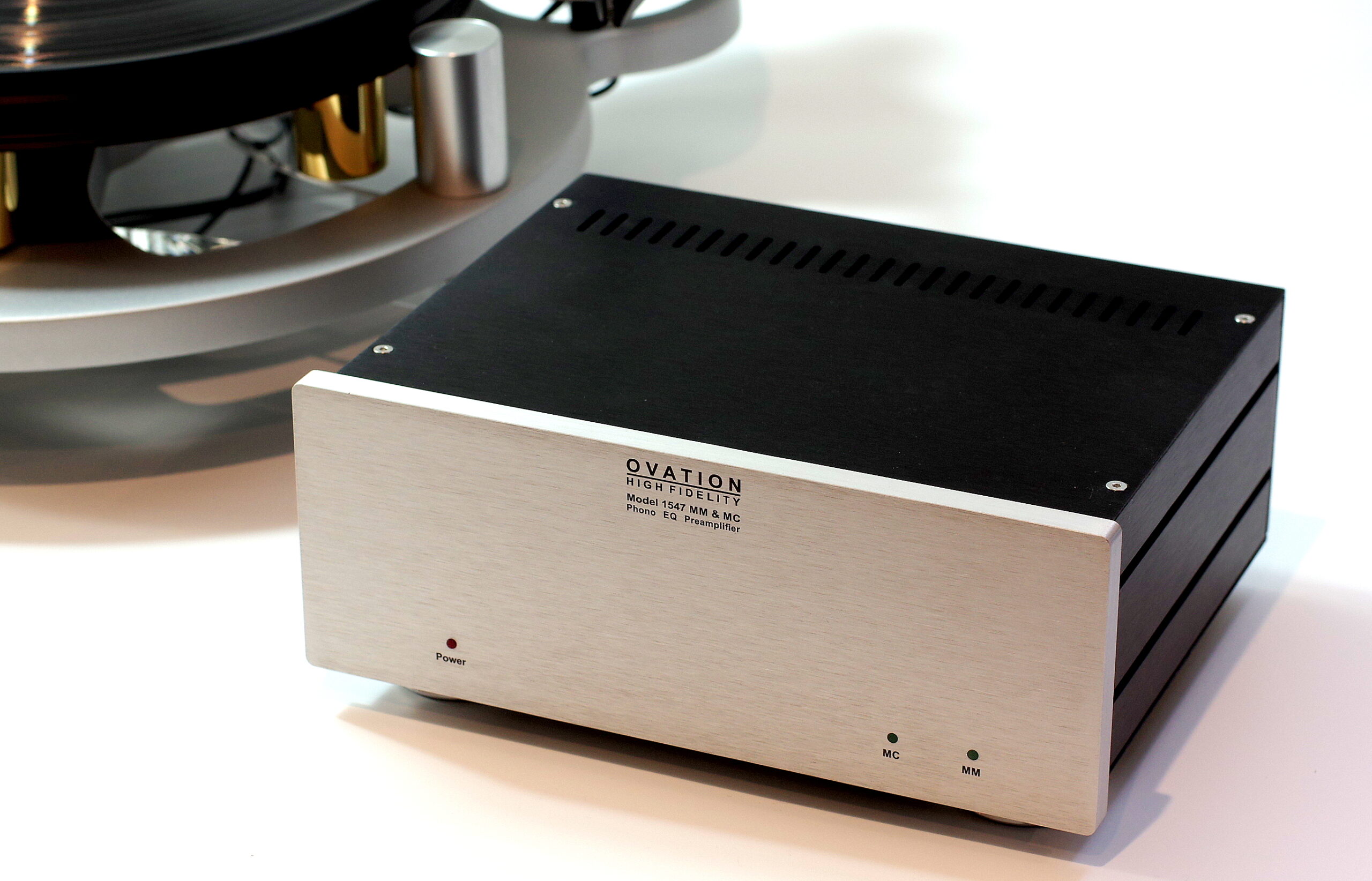
Here are some commercial products that use the techniques described in the presentation: www.ovationhifidelity.com
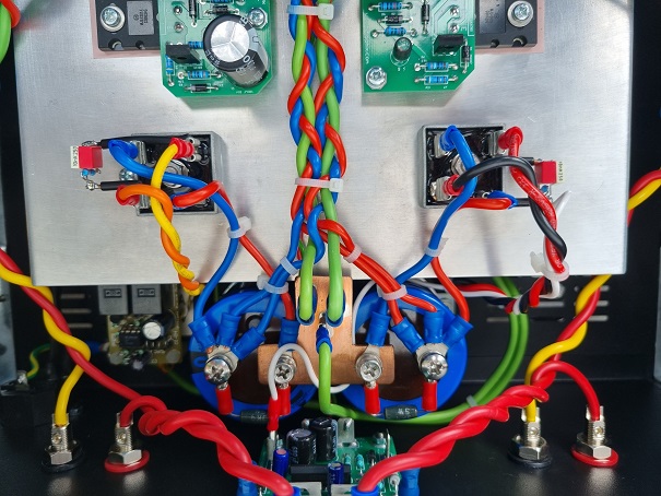
The picture below shows the internal wiring of one of the two nx-Amplifiers I built a few years ago with zero noise or hum problems. The power wiring is tightly bundled, and small signal wiring is kept well away from the transformer and other power wiring. On the PSU PCB, strict attention to the capacitor ‘T’ connection and ‘star’ ground return result in an exceptionally quiet amplifier.

Finally here is a YouTube video of HOW NOT TO DEAL WITH GROUND LOOPS. What is really disconcerting about this is that if you type ‘Ground Loops’ into Google, this will probably be the first reference that comes up on the list.
All the basic safety rules about earthing [grounding] by using a ‘ground lifter’ are completely broken and the noise problem has actually not been solved – they have gone around the problem and made the product completely unsafe in the process – and especially so since this is on a tube amplifier.
The question to ask when dealing with a potential safety fault is ‘What would happen if the live wire came loose and touched on the input jack, or any other metalwork on the product without the safety earth[ground] connected?’ If the answer is ‘it would be at the live potential’ don’t do it!
Never, ever, use a ground lifter in the manner shown in the YouTube video to get rid of hum – its plain dangerous and illegal. Period.
-
MC Head Amp Circuit Compendium
Here is the new updated moving coil head amp designs compendium – updated 31 July 2019. The first file is a PDF compendium of about 28 different circuits with noise, distortion and current consumption details. All the LTspice sim files are zipped in the second file.
What is immediately apparent from this is that having an amplifier that is much quieter than the source resistance gives little benefit.
The table below shows how the amplifier noise and the source resistance noise add. Select your amplifier equivalent noise resistance on the y axis, your source resistance on the x axis and the intersection is the total equivalent input noise. Note, as is the table does not account for input noise current – but this should not be an issue with head amps that use 1 or 2 bipolar transistors for the amplifier stage.
For example, if the source resistance is 40 Ohms, a very quiet amplifier with an equivalent input noise voltage of 2 Ohms (something like the Hawking designed by Richard Lee in the presentation above) offers only about 1/3rd lower total system noise (0.83nV/rt Hz) noise than an amplifier with an equivalent input noise of 40 Ohms i.e. 1.15 nV/rt Hz.
On the other hand, if the source resistance is just 2 Ohms, but the amplifier equivalent noise resistance is 40 Ohms (akin to a JFET input stage), the difference is far more marked and the total system noise will be about 3.2x worse than the source resistance noise.
So, as a general rule we can say:- If the amplifier equivalent noise resistance is not more than 1.414x the source resistance noise, it will be just audible since the human ear can just about detect 1.5 dB change in power level.


-
Hifisonix Ripple Eater PSU for the sx and kx-Amplifiers
The PCB’s are through hole plated and silk screened and are available from Jim’s Audio here:
Ripple Eater PSU for kx and sx Amplifiers
(please note these PCB’s are not available from the Hifisonix Shop)
Here is an Excel file with the BOM: Ripple Eater PSU BOM
The BOM is provided for assistance – always carefully check the part numbers and quantities before ordering.
Here is the BOM if the link above does not work

Introduction
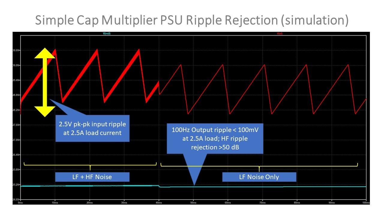
Here is a very simple capacitor multiplier PSU aka ‘ripple eater’ for the sx or kx-Amplifiers. The LTspice simulated ripple rejection at 100 Hz is about 65dB and at 10 kHz it is 85 dB. These figures assume you have a 2.5A load and also include the on-board filter capacitors on the amplifier modules themselves (220uF per rail on the sx-Amp and 1000uF per rail on the kx-Amp per amplifier module).

Class A amplifiers draw heavy quiescent current from their power supplies, and this gives rise to significant amounts of mains related ripple that will affect the amplifiers noise performance. VFA amplifiers generally have better LF PSU noise rejection than CFA’s, but it can still be a problem with a class A VFA.
A further benefit of this supply is that the radiated mains noise from the PSU to amplifier module wiring is greatly reduced because you will be supplying close to DC into the amplifier module local reservoir capacitors, so the associated mains ripple charging currents are very low. Low frequency (because the HF currents will be provided by the local on board reservoir capacitors – 220 uF for the sx-Amp and 1000 uF for the kx-Amp) signal related currents will still be flowing in the wiring of course, so you have to pay careful attention to layout, how you dress the wiring, loop area minimization and common impedance coupling issues – you can read more about this in ‘How to Wire -up a Power Amplifier’. Nevertheless, this PSU goes a long way to making sure your finished amplifier can be as quiet as theoretically possible. When combined with the 50~60dB mains noise rejection of the actual amplifiers themselves, the noise levels on the amplifier output will be down as much as 100 dB which is an outstanding result by any measure. At HF, the performance will be even better, and that is important for the amplifier sound in the mid and high range.

The series pass transistors (8A MJE15032/33 devices) are designed to be mounted underneath the PCB with their tabs screwed to the amplifier chassis base using the appropriate thermally conductive insulator (same mounting technique as the main rectifier D4 as well but you do not need the insulating washer on the rectifier – only some thermal grease). Each pass transistor will dissipate about 10W in a stereo set-up delivering full output power into the loudspeaker load.
In normal operation, you will drop ~2 volts across each pass transistor, so if you want an output of say +-27 V, the loaded DC voltage into the PSU should be 29 V. Note carefully as well, this power supply does NOT regulate the output – it will track the raw filtered DC voltage, but remove the ripple hence the ‘ripple eater’ name.
How Can I use Ripple Eater PSU on class AB Amplifiers with Higher Supply Voltages?
You can use this ripple eater power supply as is up to +-35V. You can also use it on amplifier with higher supply voltages up to +-50V. However, you must change the filter capacitors to 50 or 63V types (this is C1 and C6 in the schematic). In a class AB amplifier, you can use values that are about 3x LOWER than you would on a class A amplifier – so about 15 000 uF at 50 or 63V would be correct. You must also change C5 and C7 to 50 or 63 Volts. Finally, change R5 and R6 to 10k each. Note that the Ripple Eater PSU is not suitable for amplifiers with power supply rails much above +-50V because the series pass transistors (Q1 and Q3) are rated at 8A continuous and this places an upper limit on the output power.
Can I Increase The Power Handling Capability of the Ripple Eater?
Yes – you can.
Replace Q1 with an NJW3281 or a MJW3281
Replace Q3 with an NJW1302 or MJW1302
The PCB mounting holes for Q1 and Q3 will NOT accept the larger types above, you must run short wires from the PCB to the larger suggested power transistors above. Do not mount the offboard transistors more than 10cm away from the PCB. Make sure the transistors have a good heatsink – again, I recommend you mount them to the chassis if it is constructed of 3mm thick or more aluminium.
Remember, the transistor collectors must be insulated from the chassis – use a suitable silicon heatsink pad
Performance
The graphic at the top of this post gives some indication of the performance (simulated) of the ripple eater supply. I used a ripple eater on the e-Amp to clean-up the supply to the amplifier front end and got better than 40 dB ripple rejection improvement, so the technique works extremely well in practice. In the simulation below, for the first 40 ms, both LF and HF noise are presented to the input, and for the remaining 60 ms, just LF noise is presented. The aqua trace at bottom is the output and as you can see, the LF and HF noise is significantly attenuated.
A Word of Warning
There is a considerable amount of energy stored in the capacitors and there is NO CURRENT LIMITING on the ripple eater output. If you accidently short the output of the power supply, the series pass transistors (Q1 and Q3) will blow up in spectacular fashion. So, exercise caution when wiring up!
Secondly, remember the series pass transistors are rated at 8A – so they are not designed to supply full load current into a 4 Ohm load with continuous sine wave testing both channels driven – they will pop if you do this. If you want to do full load continuous wave testing, short out the collector to emitter on Q1 and Q3. Once testing is complete, remove the short.
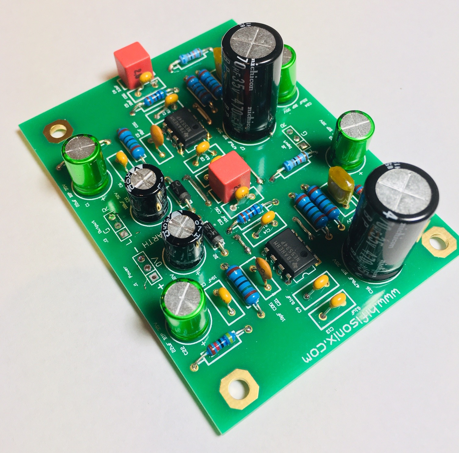
Component Overlays, Assembly and Some Pictures
Here is the component overlay for the PSU.

Below are some pictures of the finished board. Note carefully how the main bridge rectifier (D4) and the series pass transistors (Q1 and Q3) are mounted underneath the board and lay flat on the amplifier (metal) chassis.
ATTENTION!
YOU MUST USE AN INSULATING THERMAL WASHER BETWEEN Q1 AND Q3 AND THE AMPLIFIER CHASSIS!
You do not need to insulate D4 from the chassis as the thermal pad on the underside of the device is electrically isolated from the internal diodes – you must use thermal grease however to thermally couple it to the chassis – it will overheat and fail if you don’t. Remember to check with a DVM to see that there is no continuity between the chassis and the series pass transistor collectors.
Further Notes on Heatsinking/Thermal Management
If your chassis base plate is made of aluminium of at least 3mm thick, you can mount the Ripple Eater PSU as suggested above. If however your chassis is made of steel, it probably wont be too efficient at dissipating the pass transistor heat, so its best then that you use a separate heatsink and mount the devices to that. Here is a suitable one from Mouser Aavid 3.7C/W Heatsink
If you do mount the series pass transistors (Q1 and Q3) off-board, remember to twist the base, collector and emitter wires from the PCB to the heatsink mounted transistors and keep them as short as practicable (avoid going much above 10cm if you can).


You must use 8 or 10mm stand-off’s – not longer. Suitable Mouser Pt# 534-24337 or 534-24433 or 534-24443. In Europe, you can try RS components 280-9023 (expensive) or Reichelt in Germany DI 10 (best price)

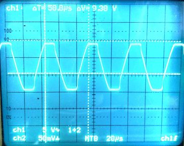
Here are some photos of the ripple eater in action. In this set-up I am running the kx-Amp off 33V rails with 400 mA per channel standing current. I used 33 000 uF capacitors (the 47 000uF were not available). The voltage drop across the series pass transistors (Q1 and Q3) with 800 mA total load current is 1.66V
This is the input voltage and the 100 Hz ripple is about 1.5V pk~pk

This next shot is the output of the ripple eater, and shows virtually no noise – the scope vertical scale is the same at 500 mV/div.

The final shot below zooms in on the ripple (vertical scale is now 20 mV/div) and we see it is in fact about 14 mV pk~pk, which is a reduction of 40 dB and there are far fewer HF harmonics in the remaining (very low) ripple.

-
How to wire-up a Dual Mono Bloc Amplifier
A few people have asked about wiring up a dual mono amp aka dual mono bloc. In a dual mono bloc there are separate power supplies and lots of opportunity for cross channel ground loops and ordinary ‘classic’ ground loops as well.
This wiring scheme addresses the situation were unbalanced connections between the source equipment and the dual mono bloc is used and should allow a dual mono amp to be wired up that is quiet – i.e. no hum.
The trick it to ensure that there is one and only one connection between the two amplifiers, and that is accomplished by bonding the input connector signal grounds together in this approach.
The wiring scheme uses two ground lifters, although you could cheat and just lift one of the amps, and ground the other directly to the chassis, but I suggest you just spend a little extra effort and use two ground lifters.
A major issue here, as in any DIY amp, is safety. Kindly note the chassis (assumed to be steel or aluminium) is bonded directly to the incoming safety ground (earth) on the IEC receptacle. You cannot under any circumstances omit this connection – it is the most important connection in DIY any amplifier. Using the ground lifters, the two amplifiers and their associated power supplies 0V then float +- 1.4V around the safety ground (earth). For the ground lifters, I always recommend you use a decent 35A 400V bridge rectifier – details in the presentation, although you can use large diodes with a high surge rating.
For the transformers, use a Toroidy (based in Poland) audio grade device with a GOSS band to minimize the radiated mag field, or if specifying custom devices, ensure your order your transformer with a GOSS band. An interwinding screen will also help to minimize mains conducted common mode noise.
One final point: there is a tendency for builders to mount the RCA input connectors on opposite sides of the rear panel. This creates a huge loop area inside the amplifier and the opportunity for a cross channel ground loop. Mount them next to each other and run the input wiring around the edge of the chassis in order to minimize the inter-channel loop areas – again, details in the presentation. -
Noise in Electronic Circuits
I’ve gathered a few articles here on noise as a go-to reference for anyone interested in the subject. These articles really focus on Johnson noise and not induced noise which is discussed in depth in the ‘Ground Loops’ post elsewhere on this site. I will update this post with new material as and when it becomes available.
-
Very Simple, Accurate RIAA Phono EQ Amp
 Very High Quality Silk Screened PCB’s for this project are available from Jim’s Audio here:-
Hifisonix RIAA Amplifier
Here is a simple no-nonsense, accurate RIAA equalizer amp you can easily build. The design uses an all-active topology and is based around an NE5534A low noise opamp. I make no claims for originality but you wont find any voodoo engineering, fairy tales or outrageous claims: It simply does what it says it does in the specification.
A complete stereo board can be built for about £25 ($35), but probably less.
The article provides some background information on the RIAA EQ standard, launched in 1954, and why it came to be the de facto industry standard after about 1960.
To use the PDF PCB layouts below, you must print the documents out on A4. Measure the reference line lengths to make sure they match. You printer should be 600 DPI resolution or better. However, I strongly recommend you just buy the PCB’s from Jim’s Audio – link above. These are very high quality boards, silk screened and gold flashed.
Overlay and 1:1 PDF negative and positive for the EQ board: Hifisonix Phono EQ Amp for Doc114
Optional PSU Overlay and 1:1 PDF positive and negative: Hifisonix Phono EQ PSU106
Gerbers for both the EQ amp and the PSU Hifisonix RIAA EQ Gerbers Hifisonix RIAA PSU Gerbers
Any questions, feel free to email me.
Can I use other op-amps with the Hifisonix RIAA?
Yes, you can. I recommend that you use unity gain stable devices with will not require an external compensation capacitor, unlike the NE5534 used here. You must first REMOVE C2 and C21 – these are the 10pF compensation capacitors. The number of good opamps in 8 pin plastic DIP packages (PDIP or mini-DIP) is unfortunately not what it used to be, so you may have to use a SMD to PDIP adaptor if you want to go down this route.

The plots below are for HIGH gain.
The plot below is of the RIAA noise and distortion at 500mV output at 1 kHz A weighted. This was with board on the workbench, no screening or special precautions and the power supply located about 15cm away. In a metal housing, you can expect about a 30 dB reduction in the 50/60Hz noise. There is quite a bit of noise being picked up from the surrounding CFL lamps etc, but the distortion is almost entirely 3rd harmonic (at -70 dB), with a bit of 5th at about -85 dB.

The plot below is the frequency response after the source signal is passed through a very accurate inverse-RIAA network. The white noise frequency response measurement technique used eliminates extraneous noise sources and is therefore extremely useful. It works by looking at the power spectral density of the amplifier output, which for a white noise source, is constant per octave. If the amplifier response (after passing through the inverse RIAA) is indeed flat, then the overall response will be flat. The A-D was set to 24bits /192 samples per second and the response display set to 30Hz to 100kHz. The RIAA conformity is excellent with no HF peaking and starts dropping off cleanly beyond about 30 kHz.

-
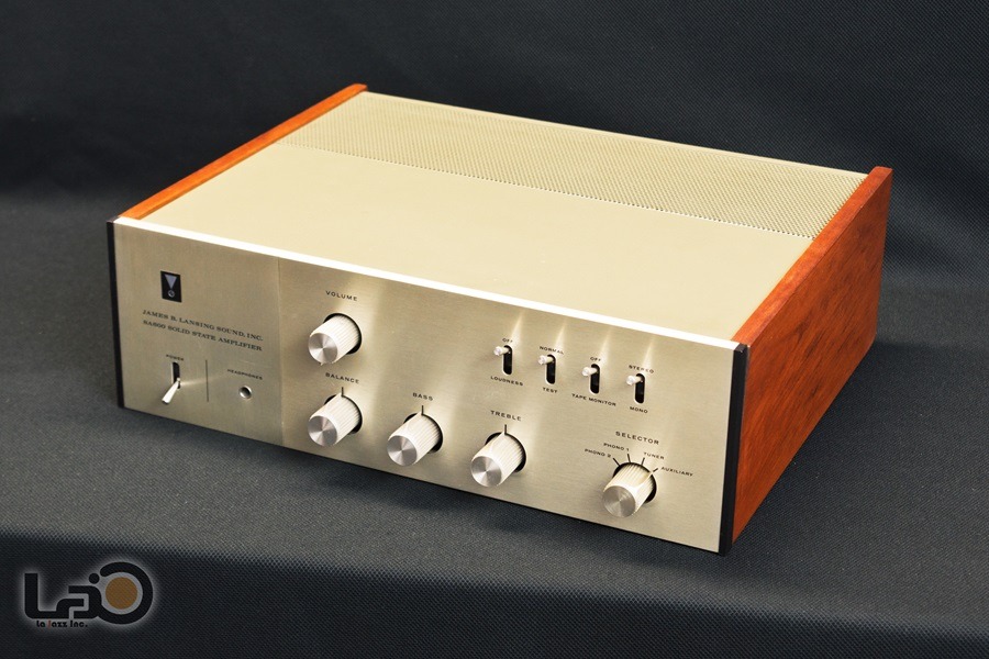
Amplifier History: The JBL SA-600

The beautifully styled JBL SA-600 amplifier was launched by the James B. Lansing company in 1966, and Bart Locanthi (the designer) wrote the technical article (link further down) in January 1967. This is one of the earliest – if not the earliest – example of a commercial amplifier that addressed the potential for TIM/SID and that of Large Signal Non-linearity (LSN).

In the mid 1960’s, most engineers were still working with tubes which had low loop gains and were not equipped to deal with the wider bandwidths, higher loop gains and attendant phase shifts that multi-stage solid state amplifiers offered. However, the SA-600 designer, Bart Locanthi, had cut his teeth on military guidance systems in the 1950’s – the heyday of the analog computer – and would have been, as I have remarked elsewhere on this site, highly cognisant of things like slew rate, slewing distortion, loop gain, phase margin, overshoot and so forth. Unusually for the time, the front end diff pair (Q7 & Q8) is degenerated and loop compensation provided by an 82 Ohm and 150 pF resistor across their collectors along with a 220 Ohm and 75pF network from the VAS output to ground. It operates in inverting mode, which has been tried on numerous commercial amplifiers over the years (the modern take on this is that non-inverting mode offers advantages with respect to noise performance). This design delivered 30 Watts RMS per channel, which was more than enough for the efficient loudspeakers of the day, and quite in line with the general power levels on offer from tube based gear.
Locanthi’s EF3 output stage, nicknamed the ‘T’, has remained the go to circuit for high performance solid state amplifiers – it features wide bandwidths, very high current gain, and can easily be scaled up by adding output transistors in parallel. Because of the high gains involved, care is needed in layout along with good local decoupling. Although we do not have the rest of the power supply details, it seems this was well taken care of along with the base stoppers preceding Q3 and Q4.

Bart Locanthi Nowadays, we would do things a little differently insofar as compensation goes (for example, the VAS would not be loaded to ground), and the VAS would certainly be loaded with a current source in the manner described by Douglas Self’s ‘blameless’ amplifier. Nevertheless, this design is a classic and was years ahead of its time in a number of very important aspects. Otala’s paper on TIM was still a few years away and he would regrettably draw the wrong conclusions from his findings i.e. that TIM is the result of feedback. We now know this is emphatically not the case – its all about how it is applied.
It should be remembered that solid state devices were still in their infancy, and very expensive compared to todays prices – this required some creative engineering to minimize costs and still end up with reasonable performance which this design certainly does.
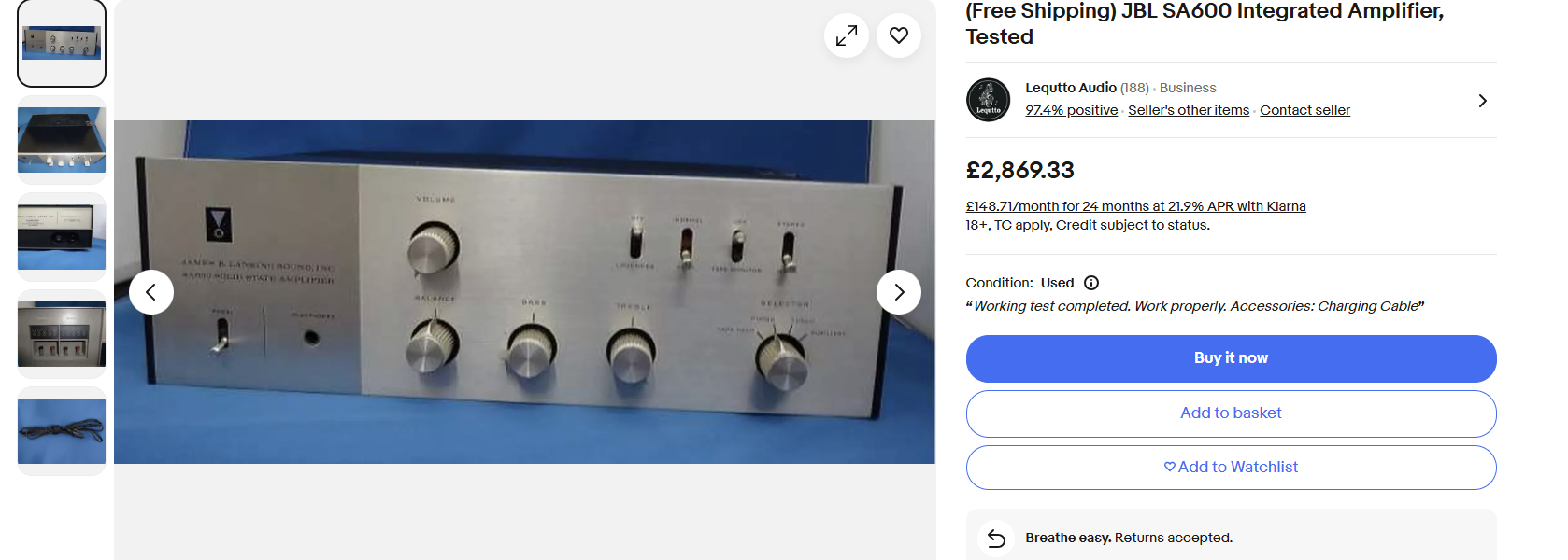
However, the other fascinating thing about this amplifier is that it has held up its value remarkably – a bit like a Rolex watch. If you root around on eBay or any of the pre-owned hi-fi websites, you are unlikely to pick up a cosmetically good working unit for less than about $2000 (!) and I’ve seen immaculate exemplars for sale at over $4000 (eBay Japan). So, highly regarded in its day for its liquid tube like sound, and still sought after as a collector’s piece – which just goes to show that a well-engineered product – be it solid state or tube – can hold its value for decades and still deliver an outstanding listening experience when partnered with sympathetic ancillary gear.
You can read Locanthi’s original description of his design below :-
Here is a short review of the amplifier done in 1966 by Julian Hirsch
JBL – SA-600 Stereo Amplifier (J.D.Hirsch) (1966)
A vintage JBL SA600, recently restored for a member of Audio Science Review, underwent technical assessment by the ‘Chief Fun Officer’, Amirm. While the restoration was extensive, my analysis suggests the amplifier still exhibits residual faults. Specifically, the measured level of hum and noise, even by 1966/67 standards, would have been considered unacceptable for a product of this calibre. Modern, well-engineered amplifiers will surpass the JBL SA600 in terms of absolute hum, noise floor, and distortion levels and this simply reflects the maturation of audio design, where knowledge has disseminated widely since the SA600’s era.
Despite these observations, reviewer Amirm acknowledged the amplifier’s performance considering its 60-year vintage. Notably, Julian Hirsch’s original review cited measured hum and noise figures exceeding -100 dB, a remarkable achievement. In my view, this discrepancy suggests the restored unit tested by ASR may still harbour unresolved issues. At the time, the SA600 competed primarily with tube amplifiers, which exhibited higher noise, hum, and distortion while delivering significantly less power than the SA600’s conservatively rated 30 to 40 watts, as noted by Hirsch.
Interestingly, the placement of input and power connectors on the amplifier’s bottom chassis reflects the prevailing audio system design of the time. In an era where systems were often integrated into wooden consoles, this configuration facilitated efficient cable management.


